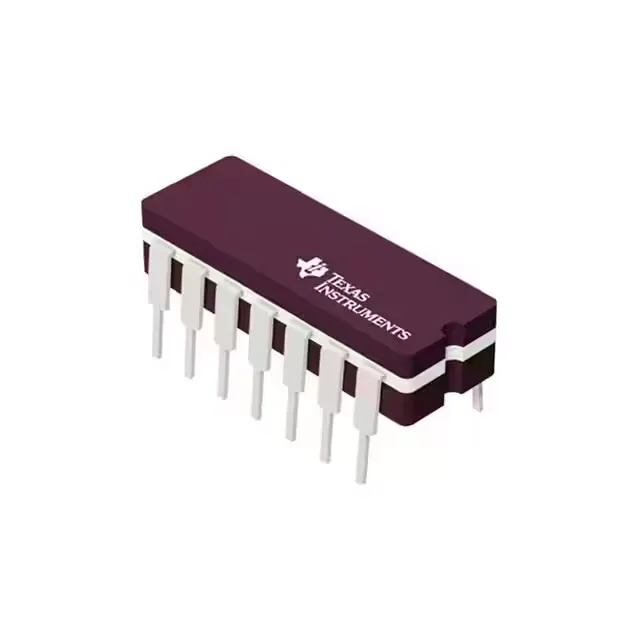
Active 74LS quad AND gate — BOM-fit note
The SN74LS08N is an active-production Texas Instruments quad 2-input AND gate from the 74LS Schottky-clamped TTL family. Four independent gates in a single 14-pin DIP — each gate takes two inputs and drives a single output high only when both inputs are high. The 74LS series runs cooler than plain 74 TTL but still needs the 5 V rail held within 5 %. Operating temperature is 0 °C to 70 °C, so it is a commercial-grade part — fine for a benchtop or indoor panel, not for an engine bay or freezer.
20 ns propagation delay — timing and fan-out limits
Max propagation delay is 20 ns at 5 V with a 15 pF load. That sets the data-rate ceiling — at 20 ns per gate, a two-level AND-OR chain adds 40 ns of combinatorial delay before the clock edge. For a 10 MHz clock (100 ns period), that is 40 % of the cycle eaten by logic, leaving little setup margin. Output drive is asymmetric: 400 µA sourcing high, 8 mA sinking low. The high-level drive is weak — fan-out to other LS loads is about 10 inputs per output. Driving a CMOS input or a long trace may need a pull-up or a buffer. The low-level sink is generous for TTL; it can drive a standard LED (with a series resistor) or a relay coil through a transistor base. Input logic thresholds are 0.8 V low and 2.0 V high — standard TTL levels. A 3.3 V CMOS output driving this gate needs a level translator or an open-drain pull-up to 5 V, because the 3.3 V high at 2.8 V barely clears the 2.0 V threshold and leaves no noise margin.
14-DIP through-hole — rework bench perspective
The 14-pin DIP (0.300-inch row spacing) is about as rework-friendly as logic packages get. Pin pitch is 2.54 mm — you can probe every pin with a scope tip, and a standard IC extractor lifts it cleanly from a plated-through-hole board without lifting a pad. The 7.62 mm body width means no tight clearances to adjacent components. Through-hole mounting means the part survives repeated soldering cycles — desolder with a vacuum station or solder wick, reinsert, and reflow. No moisture sensitivity level to track, no hot-air profile to tune. The 14-PDIP supplier device package is the same mechanical outline as the standard 14-pin DIP; any socket or footprint that takes a 0.300-inch DIP works.
Sourcing posture and compliance
The 74LS series is a mature logic family — TI has produced it for decades. No official successor or second-source cross-reference is listed; the part is the original design-in choice for 5 V TTL systems. For new designs, the 74HC or 74LVC families offer lower power and wider supply range, but the 74LS remains the drop-in replacement for existing boards.