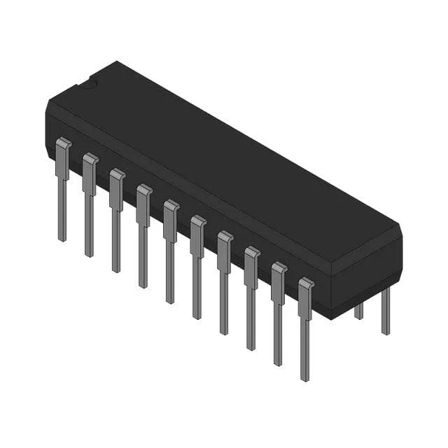
8-bit D-type register with inverted tri-state bus drive
The SN74HCT564N is an 8-bit D-type flip-flop from the 74HCT logic family, packaged in a 20-pin DIP (0.300" body) for through-hole assembly. It clocks data on the positive edge of the clock signal and presents the stored state as inverted outputs through a tri-state buffer — the bus stays high-impedance when the output-enable pin is asserted, letting multiple registers share a common data bus without contention. The 50 MHz maximum clock frequency and 35 ns propagation delay (at 4.5 V, 50 pF load) set the timing budget for the data path — the 35 ns figure includes the clock-to-output delay plus the output rise time into the capacitive load, so the actual setup-and-hold window at the receiver is tighter than the raw propagation number suggests.
Temperature grade and supply rail — what the ratings mean for fit
A board that lives in an outdoor enclosure, engine bay, or cold-chain environment stays within the rated junction temperature without derating the clock speed or output current. If the upstream controller drives 3.3 V CMOS into the clock or data inputs, the input threshold (typically 0.8 V for low, 2.0 V for high at 5 V) may not cross the high-level minimum — a level translator or open-drain buffer is needed between the domains.