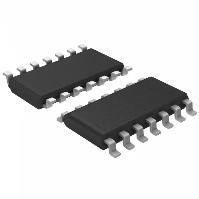
14-SOIC quad AND gate with open-drain outputs
The SN74HCS09DR is a Texas Instruments 74HCS-series quad 2-input AND gate in a 14-SOIC package (0.154" body width, 3.90 mm). Each of the four independent gates combines two Schmitt-trigger inputs with an open-drain output — the output pulls low when the AND condition is met and floats high when it is not, which lets multiple gates share a common pull-up or drive a wired-OR bus. The 2 V to 6 V supply range covers both 3.3 V and 5 V logic rails, and the -40°C to +125°C operating temperature matches industrial and automotive under-hood environments where the standard 74HC family's 85°C ceiling would be marginal.
What the open-drain output and Schmitt inputs mean for the bus
The open-drain output sinks 7.8 mA when active (V_OL) and floats to high impedance when the gate is off — it cannot source current. This means the output high level is set entirely by the external pull-up resistor and supply rail, making the part suitable for level translation (e.g., a 5 V gate driving a 3.3 V pull-up domain) or for wired-OR connections where multiple outputs share a single pull-up without contention. The Schmitt-trigger inputs accept slow or noisy edges without oscillation: the low-level threshold ranges from 1 V to 3 V, and the high-level threshold from 1.5 V to 4.2 V, giving typical hysteresis of about 1.2 V at 5 V supply. This cleans up signals from mechanical switches, long PCB traces, or RC-delay networks before the AND logic evaluates them.
Timing and power budget for the BOM
Maximum propagation delay is 11 ns at 6 V supply with a 50 pF load — at 3.3 V the delay is longer (not specified here, but typical for the 74HCS family). For a 10 MHz clock or data path, the 11 ns gate delay plus the open-drain pull-up rise time (set by the RC time constant of the pull-up resistor and load capacitance) must fit within the timing budget. Quiescent current is 2 µA max across the full supply range — the gate draws nearly nothing when the outputs are static. The dynamic current depends on the switching frequency and the load capacitance being charged through the pull-up resistor (the open-drain output only sinks, so the pull-up carries the charge current).
Active lifecycle and sourcing posture
The 14-SOIC package (supplier device package 14-SOIC) is a standard JEDEC outline with 1.27 mm lead pitch — it fits the same footprint as other 14-pin SOIC logic gates, simplifying board layout if a pin-compatible alternative is needed.