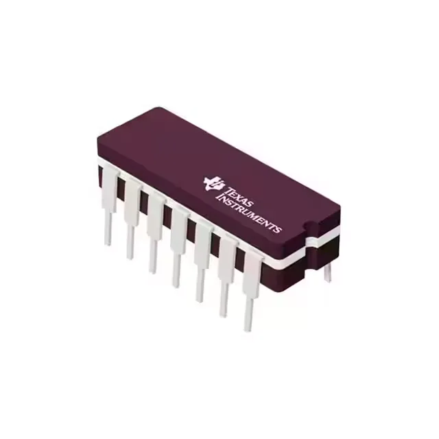
Texas Instruments SN74HC32N — Analog & Data Acquisition

SN74HC32N Texas Instruments OR Gate, 4-ch 2-in, 14-DIP

MPNSN74HC32N
End of Life

Texas Instruments 74HC series OR Gate, 4-circuit 2-input, Through Hole 14-DIP (0.300", 7.62mm), Tube, 2V ~ 6V supply, -40°C ~ 85°C, SN74HC32N.

$0.6Ref. price · indicative, final on quote
Packaging14-DIP (0.300", 7.62mm)
StockContact for availability
Lead timeIn Stock wk
MOQ1 pcs
  • 100% new & originalTraceable channels only — no refurbs, no pulls, no remarked parts.
  • Date & lot codes on quoteStated per line before you commit; label photos on request.
  • MSL-compliant ESD packingMoisture-sealed bags with indicator cards; reels photo-verified.
  • PayPal buyer protectionPay by T/T, PayPal or Payoneer — card payments covered end to end.

Specifications

SN74HC32N Technical Specifications
ParameterValue
Series74HC
Logic typeOR Gate
Mounting typeThrough Hole
Voltage2V ~ 6V
Current - quiescent2 µA
Current - output high, low5.2mA, 5.2mA
Number of inputs2
Operating temperature-40°C ~ 85°C
PackageTube
Case14-DIP (0.300\", 7.62mm)
Number of circuits4
Input logic level - low0.5V ~ 1.8V
Input logic level - high1.5V ~ 4.2V
Max propagation delay @ v, max CL17ns @ 6V, 50pF

Product details

Quad 2-input OR gate in 14-pin DIP — BOM-fit for 5V logic

The SN74HC32N is a Texas Instruments 74HC-series quad 2-input OR gate in a 14-pin through-hole DIP package. It operates from a 2V to 6V supply, making it a direct fit for 5V TTL-compatible logic rails as well as 3.3V mixed-voltage boards. Each of the four gates sinks or sources 5.2mA of output current, which is enough to drive one or two standard CMOS loads but not a high-fanout bus — budget a buffer stage if the output needs to drive more than a few pF of trace capacitance. Propagation delay is 17ns max at 6V with a 50pF load, so the gate can toggle at roughly 30 MHz in a clean layout. That speed is adequate for control logic, address decoding, and general-purpose gating in sub-20 MHz clock domains.

Active production — sourcing and compliance

The 14-DIP package (0.300" body width) is the standard through-hole footprint — no adapter board needed for breadboard or prototype builds. Quiescent current is 2 µA max, so the gate adds negligible standby draw in battery-powered designs. The input logic levels (low 0.5V–1.8V, high 1.5V–4.2V at 2V–6V supply) are compatible with most 3.3V and 5V CMOS outputs without external level shifting.

Frequently asked questions

What is the closest functional second-source for SN74HC32N?

The SN74HC27APWR is a 74HC-series triple 3-input NOR gate in a surface-mount package — it is not a pin-compatible drop-in for the SN74HC32N. The SN74HC32N is a quad 2-input OR gate in a 14-DIP through-hole package; the SN74HC27APWR is a triple 3-input NOR gate in a TSSOP package. For a direct OR-gate replacement in the same DIP footprint, the SN74HC32N itself is the only active 74HC-series quad 2-input OR gate in that package from TI.