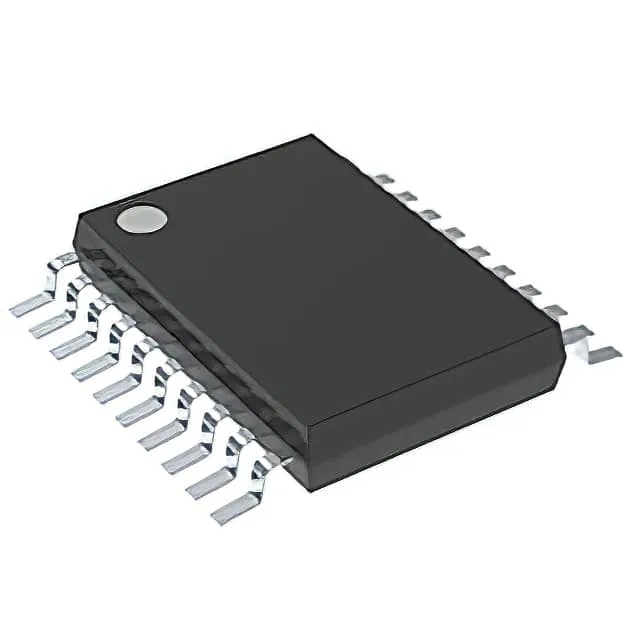
Bus switch identity and circuit configuration
The SN74CBT3345PW is an 8-bit bus switch from the 74CBT family, configured as 8 independent 1:1 SPST switch channels. Each channel presents a low on-resistance path when the output-enable pin is asserted, effectively connecting the A and B ports with propagation delay under 250 ps — the switch is transparent to the data rate up to the bandwidth limit of the pass transistor. The single-supply architecture means the switch passes signals between 0 V and Vcc; it does not level-translate, so both sides of the switch must operate within the same voltage domain.
20-TSSOP footprint and board integration
Housed in a 20-pin TSSOP (4.40 mm width, 0.65 mm pitch), the SN74CBT3345PW mounts on the same land pattern as the standard 20-TSSOP footprint shared by many 74-series logic parts. The 0.65 mm pitch is routable on a two-layer board with 6/6 mil trace/space rules — no micro-via or blind-via stack-up required. The supplier device package designation 20-TSSOP matches the JEDEC MO-153 variation; confirm the PCB footprint matches the package drawing before committing the BOM position. Supplied in tube packaging (50 units per tube typical for TSSOP-20).
Active production and compliance status
Because the 74CBT family is a mature logic series with multiple second-source vendors (Nexperia, ON Semiconductor, Diodes Inc offer functionally equivalent 74CBT parts), a BOM hedge is straightforward — the 20-TSSOP footprint and 4.5-5.5V supply rail are industry-standard. Confirm the specific output-enable logic polarity and channel count match the design before substituting a different vendor's order code.