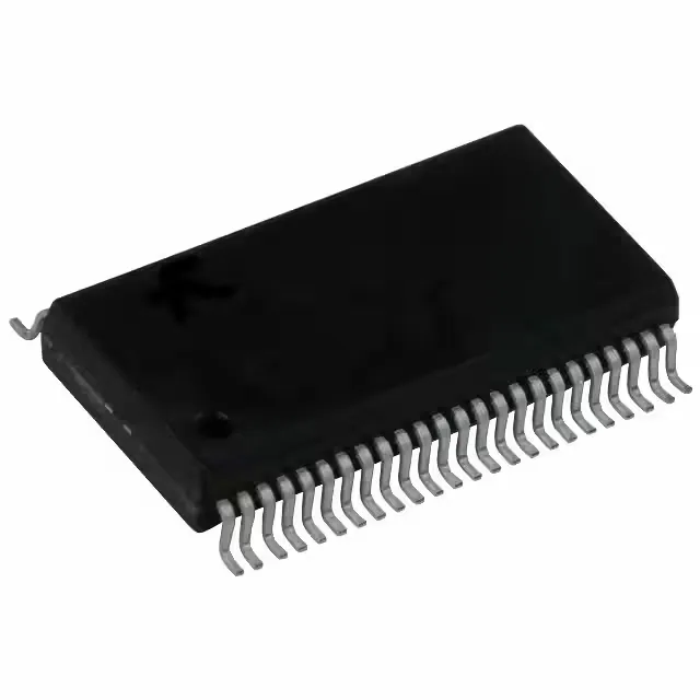
16-bit bus buffer for mixed-voltage logic
It operates across a 1.4V to 3.6V supply range, making it a natural fit for designs that bridge 1.8V, 2.5V, and 3.3V logic domains without a separate level translator. Organized as four independent 4-bit elements, it handles 16 bits of bus buffering in a single 48-pin TSSOP package.
The 1.4V to 3.6V supply covers the three most common digital logic rails: 1.8V, 2.5V, and 3.3V. If your board has a 1.8V FPGA bank driving a 3.3V peripheral, this buffer sits between them and runs from whichever rail has the headroom. The wide range also gives margin for a regulated 3.3V rail that droops under load — the buffer keeps working down to 1.4V without corrupting the bus.
Output drive and temperature grade
Each output sources or sinks 12mA, which is enough for standard CMOS loads, short PCB traces, and typical bus fan-out of four to eight loads. For automotive or under-hood use, you'd step to the AEC-Q100 variants in the 74AVC family.
The 48-TSSOP (6.10mm body width) is a fine-pitch, 0.5mm-lead-pitch package. A hot-air station at 280°C with a small nozzle lifts it cleanly — just tack the corners first.