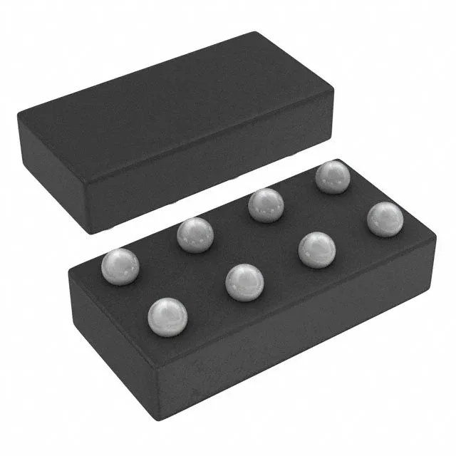
8-DSBGA footprint and board-level integration
The SN74AUP2G80YFPR comes in an 8-XFBGA, DSBGA package (supplier device package 8-DSBGA) — a 0.5 mm pitch wafer-level chip-scale package that routes the two flip-flop channels into a 1.5 mm² footprint. The exposed solder balls demand a controlled stencil aperture and a micro-via-capable PCB stack-up; the narrow pitch rules out hand-assembly and makes X-ray inspection the standard for joint verification. Surface-mount only — no through-hole variant exists. The package is ROHS3 compliant, so the reflow profile follows the standard lead-free ramp-soak-peak curve for SAC305 solder.
Clock speed and propagation delay budget
Rated for a clock frequency of 257 MHz, this dual D-type flip-flop toggles at a rate that suits moderate-speed data pipelines and control logic in portable or battery-operated gear. The max propagation delay is 6.4 ns at 3.3 V with a 30 pF load — that delay sets the timing margin for the downstream capture flop; at 257 MHz the period is roughly 3.9 ns, so the 6.4 ns delay means the output transition completes well within one clock cycle at lower frequencies, but at the rated maximum the setup/hold window tightens and the load capacitance must stay at or below 30 pF to meet the datasheet limit. Positive-edge triggered with inverted output — the Q-bar output inverts the D input on each rising clock edge. The dual-element configuration packs two independent 1-bit flip-flops into one package, each with its own D, clock, and Q-bar pins.
Supply range and quiescent draw for battery duty
Operates from 0.8 V to 3.6 V — the 0.8 V floor lets it run directly from a near-depleted single-cell lithium primary or a 0.9 V alkaline cell, while the 3.6 V ceiling covers the full Li-ion range. Quiescent current is 500 nA typical, so the flip-flop's own draw is negligible in a system that spends most of its time in sleep mode — a sensor node waking once per second to latch a reading burns more current in the MCU's RTC than in this flop. Output drive is 4 mA source and 4 mA sink at 3.3 V — enough to switch a CMOS gate input or a low-power LED indicator, but not a relay coil or a long PCB trace without a buffer. Input capacitance is 1.5 pF, keeping the clock-line load light even with both flip-flops driven from the same source.
Temperature grade and deployment context
Rated for -40°C to 85°C ambient — the industrial temperature band covers outdoor telecom cabinets, factory-floor sensor interfaces, and automotive cabin electronics (non-engine-bay). The 74AUP series is TI's ultra-low-power logic family, positioned below the 74AUC and 74AVC families in dynamic power; the trade-off is lower output drive and slightly higher propagation delay compared to the faster families, but for a battery-powered edge where every nanoamp counts, the 74AUP is the right choice.
Lifecycle and sourcing posture
No pin-compatible second-source or official successor is recorded — the part is a single-source item from TI.