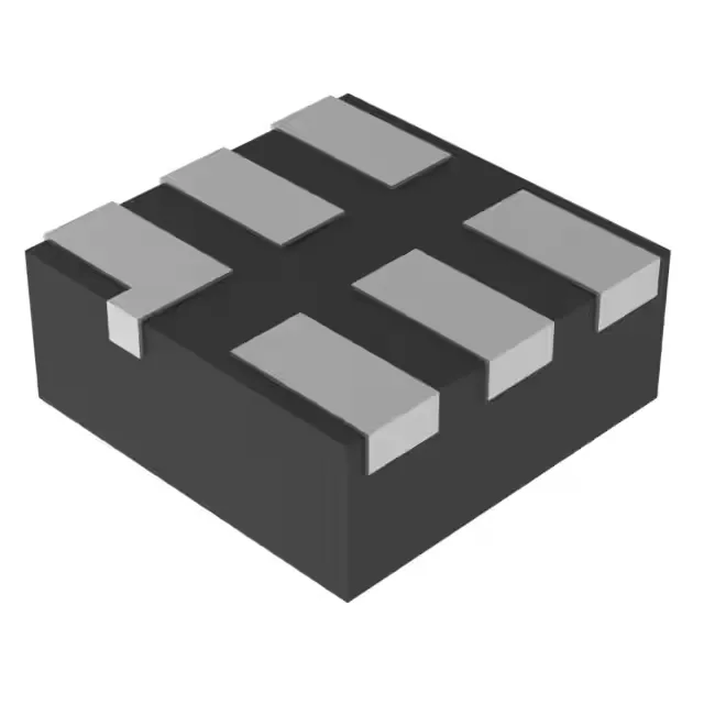
Dual buffer with Schmitt-trigger inputs in a 1x1mm SON
It operates across a 0.8V to 3.6V supply range, making it suited for battery-powered and low-voltage portable designs. Each of the two elements drives up to 4mA source and sink, enough to fan out to multiple CMOS logic inputs.
Supply voltage range and what it enables
The 0.8V to 3.6V supply span directly matches the core voltages of modern low-power MCUs, FPGAs, and SoCs. At the low end, it interfaces cleanly with 1.2V or 1.8V logic without an external level translator. At 3.6V it handles legacy 3.3V rails. The Schmitt-trigger input provides hysteresis that cleans up slow edges from RC debounce circuits, sensor comparators, or long PCB traces — a common need in panel interfaces and pushbutton inputs.
Package and layout reality
Housed in a 6-XFDFN (6-SON) package measuring 1x1mm, this part is sized for dense PCB layouts where every square millimetre counts — think wearable, IoT sensor nodes, or multi-channel interface modules. The small footprint means the board assembler needs to handle DFN-style packages; the 0.5mm pitch is standard for that class. No exposed thermal pad to worry about, but the tiny body demands precise stencil aperture for solder paste.
No last-time-buy or obsolescence risk on the horizon.