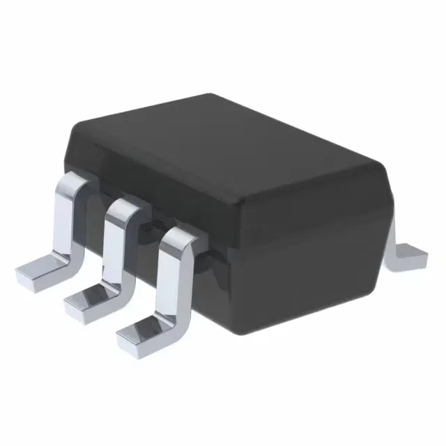
Texas Instruments SN74AUP2G04DCKR — DC-DC Power Modules

SN74AUP2G04DCKR TI 74AUP Dual Inverter, 0.8V–3.6V, SC-70-6

MPNSN74AUP2G04DCKR
End of Life

Texas Instruments 74AUP series, SN74AUP2G04DCKR, dual inverter logic gate, 2 circuits, 2 inputs per circuit, 0.8 V to 3.6 V supply, 6.2 ns propagation delay at 3.3 V, 30 pF load, SC-70-6 package, -40°C to 85°C operating temperature.

$0.61Ref. price · indicative, final on quote
Packaging6-TSSOP, SC-88, SOT-363
StockContact for availability
MOQ1 pcs
  • 100% new & originalTraceable channels only — no refurbs, no pulls, no remarked parts.
  • Date & lot codes on quoteStated per line before you commit; label photos on request.
  • MSL-compliant ESD packingMoisture-sealed bags with indicator cards; reels photo-verified.
  • PayPal buyer protectionPay by T/T, PayPal or Payoneer — card payments covered end to end.

Specifications

SN74AUP2G04DCKR Technical Specifications
ParameterValue
Series74AUP
Logic typeInverter
Mounting typeSurface Mount
Voltage0.8V ~ 3.6V
Current - quiescent500 nA
Current - output high, low4mA, 4mA
Number of inputs2
Operating temperature-40°C ~ 85°C
PackageTape & Reel (TR); Cut Tape (CT)
Case6-TSSOP, SC-88, SOT-363
Number of circuits2
Input logic level - low0.7V ~ 0.9V
Input logic level - high1.6V ~ 2V
Max propagation delay @ v, max CL6.2ns @ 3.3V, 30pF

Product details

0.8 V to 3.6 V supply — the defining range

The SN74AUP2G04DCKR from Texas Instruments is a dual inverter from the 74AUP ultra-low-power logic family. It operates across a supply range of 0.8 V to 3.6 V, making it one of the few standard logic gates that can run from a 0.8 V rail — relevant for battery-operated and energy-harvesting designs where the core voltage drops below 1 V. The two independent inverter channels each sink or source 4 mA, enough to drive a following logic input or a low-power LED indicator through a series resistor. Quiescent current maxes at 500 nA across the full temperature range, so it won't eat into a sleep-mode budget.

6.2 ns propagation delay — timing margin at 3.3 V

With a maximum propagation delay of 6.2 ns at 3.3 V and 30 pF load, this inverter keeps up with moderate-speed clock and data paths. In a 10 MHz system the 6.2 ns represents about 6% of a 100 ns period — comfortable margin for most glue-logic applications. At lower supply voltages the delay increases; the 0.8 V end of the range will see significantly longer propagation times, so timing closure should be verified at the actual operating point.

Package and footprint — SC-70-6

The part comes in a 6-pin SC-70-6 (SOT-363) package, a common small-outline footprint that fits into dense PCB layouts. It is surface-mount only, so hand-prototyping needs a fine-tip iron or hot-air station.

Lifecycle and compliance

The SN74AUP2G04DCKR is listed as Active with no end-of-life notification. It is ROHS3 compliant, so it meets current European and global restrictions on hazardous substances. The industrial temperature range of -40°C to 85°C covers most commercial, telecom, and factory-automation environments — no AEC-Q automotive grade on this variant, so it stays out of under-hood or chassis-domain designs that require the Q1 suffix.

Sourcing note

This is a current-production part from Texas Instruments, widely available through independent distribution. Pricing and stock levels are confirmed at quote time against an RFQ. For a BOM line that needs a dual inverter with sub-1 V capability and 500 nA quiescent draw, the 74AUP2G04 is a clean fit with no LTB risk.

Frequently asked questions

What is the propagation delay of SN74AUP2G04DCKR at 3.3 V?

This is the worst-case figure across temperature and process.

Is SN74AUP2G04DCKR equivalent to any other part number?

Within the 74AUP family, the closest functional sibling is the SN74AUP2G08YZPR, which is a dual AND gate rather than a dual inverter. The SN74AUP1G14DSFR is a single inverter with Schmitt-trigger inputs. Neither is a direct pin-for-pin replacement — the 2G04 is the dual inverter option in this series.