The SN74AUP1G98YFPR: RoHS3 compliant with no exemptions, so it ships fully lead-free for EU, UKCA, and global markets without special handling or documentation overhead.
Supply range and logic flexibility
Operates from 0.8V to 3.6V — this covers the full ultra-low-voltage range from a single-cell battery at end-of-discharge (0.9V) up to standard 3.3V logic rails. At 0.8V it still switches, which matters for energy-harvesting or deeply discharged coin-cell designs. Configurable multiple-function gate with three inputs and a single-ended output — the logic function is set by the input pin connections, not by an internal mask option. One part number covers AND, OR, NAND, NOR, XOR, XNOR, and inverter configurations depending on how you tie the inputs. Schmitt trigger input on all pins — the hysteresis cleans up slow edges from RC debounce circuits, sensor outputs, or long PCB traces without an external schmitt buffer.
Package reality — 6-DSBGA rework considerations
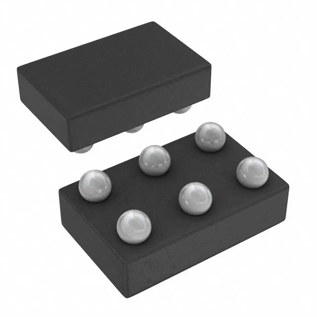
Housed in a 6-bump DSBGA (6-DSBGA) — this is a wafer-level chip-scale package with 0.5mm pitch and no visible leads. The bumps are directly under the die, so the footprint is the die size plus a few tenths of a millimeter per side. Surface-mount only — no through-hole equivalent exists. The tape-and-reel packaging (offered in both TR and CT options) suits pick-and-place assembly; hand-soldering a DSBGA is impractical without a stencil and reflow oven.
Temperature grade and output drive
Output drive is 4mA at both high and low states — typical for the 74AUP family's ultra-low-power design. This drives about four to six standard CMOS inputs; for longer fan-out or higher capacitive loads, a buffer stage is needed.