Supply range and quiescent current define the fit
The SN74AUP1G32DBVR is a single 2-input OR gate from Texas Instruments' 74AUP series — the ultra-low-power logic family. Its supply range of 0.8V to 3.6V means it runs directly from a single-cell Li-ion battery (nominal 3.6V) down to the near-depleted voltage, and also sits comfortably on a 1.8V or 3.3V digital rail without a secondary regulator. The headline number is the 500 nA maximum quiescent current. In a battery-powered sensor node that spends 99.9% of its time asleep, that standby draw is below the self-discharge rate of a CR2032 coin cell — the gate can stay powered and hold its logic state for years without draining the battery.
Speed and drive — what the propagation delay means for signal integrity
The 6.4 ns max propagation delay at 3.3V with a 30 pF load sets the data-rate ceiling for this gate in a signal path. For a 50 MHz clock or data line, that delay is about one-third of the period — the gate adds measurable skew but stays within timing margin for most glue-logic applications. At 1.8V the delay increases; the datasheet curve (not reproduced here) shows the trade-off. Output drive is 4 mA source and sink at the rated supply — enough to fan out to ten standard CMOS inputs but not to drive an LED or a relay coil. The input logic thresholds track the supply: low at 0.7V to 0.9V, high at 1.6V to 2V across the full voltage range, so the gate interprets signals correctly even when the upstream and downstream rails differ.
Package and temperature — board-level integration
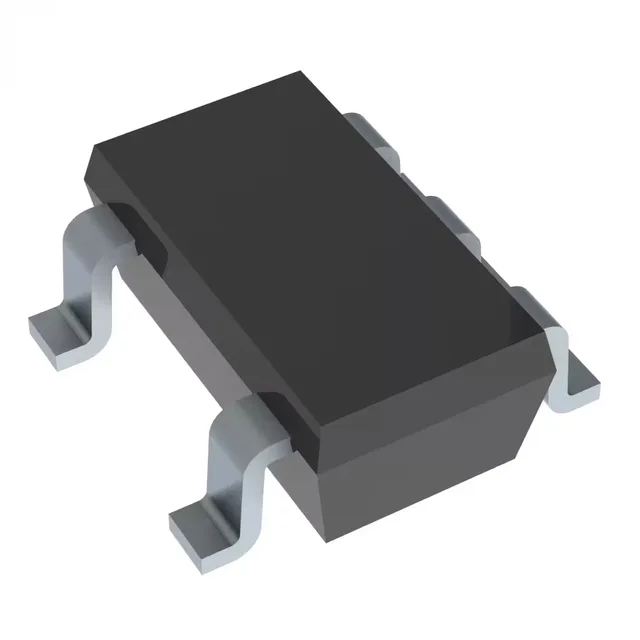
The SN74AUP1G32DBVR comes in the SC-74A / SOT-753 package, which shares the standard 5-pin SOT-23 footprint. The supplier device package is SOT-23-5 — a 2.9 mm × 1.6 mm body with 0.95 mm pin pitch. Surface-mount assembly with standard reflow profiles; the small footprint leaves room for passives on dense boards. The operating temperature range is -40°C to 85°C, covering commercial and most industrial environments. Not rated for automotive under-hood or extended 105°C+ ambient — for those, the AUP family has AEC-Q100-qualified variants in different order codes.
Lifecycle and compliance — no surprises for the BOM
Texas Instruments lists the SN74AUP1G32DBVR as Active — no end-of-life notice, no last-time-buy window. It is suitable for both new designs and production replenishment. ROHS3 compliant, with no EU RoHS exemption issues for global shipments. The part is supplied in Tape & Reel (TR) and Cut Tape (CT) options — the reel quantity suits volume pick-and-place; the cut tape works for prototype builds and small-batch assembly.