What the Schmitt trigger cleans up on a noisy rail
The SN74AUP1G14DPWR is a single inverter with a Schmitt-trigger input, meaning it reshapes a slow or noisy edge into a clean digital transition. If a board has a pushbutton, an RC oscillator, or a sensor output that rises through the threshold zone, this gate prevents the output from chattering or oscillating at the switching point. The 500 nA max quiescent current means it won't drain a battery in a portable or always-on circuit. Output drive is 4 mA source and sink at the rated supply — enough to light a small LED, drive the input of another logic gate, or toggle a MOSFET gate through a series resistor, but not a relay coil or a long cable without a buffer.
Package footprint and the layout decision
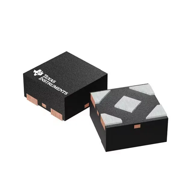
The package/case is listed as 4-XFDFN Exposed Pad — these refer to the same physical footprint; the X2SON is the TI-specific naming for the ultra-small 5-pin DFN. At 0.8 mm square, this is a hand-solder-only part without a stencil and hot air. The exposed pad needs a thermal land on the PCB, and the four signal pads are on the periphery. Verify the land pattern in the TI datasheet before committing the board — the pad geometry is tighter than a standard SC-70 or SOT-23.
Speed and signal integrity — the 6.2 ns window
Max propagation delay is 6.2 ns at 3.3V with a 30 pF load. For a 100 MHz clock buffer, that delay adds jitter and skew between branches — this gate is better suited for control signals, reset lines, and enable paths where 6 ns of propagation is acceptable. Input logic thresholds are ratiometric with the supply: low level is 0.1V to 0.8V, high level is 0.6V to 2.29V across the full supply range. The hysteresis between these thresholds (roughly 200 mV typical) is what rejects noise on a slowly changing input.
Active lifecycle and compliance standing
No alternate or second-source MPN is officially listed by TI, but the 74AUP family is widely second-sourced by other logic vendors — check the functional equivalent from Nexperia or NXP if dual-sourcing is required.