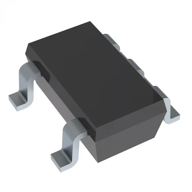
Single buffer gate for ultra-low-voltage buses
Its supply range from 0.8V to 3.6V lets it interface directly with 1.2V or 1.8V core logic without an extra level translator, saving board area and BOM cost. The 3-state output goes high-impedance when the output-enable pin is low, making it a clean choice for shared data lines or GPIO expansion on battery-operated gear.
Supply voltage — the main event
The 0.8V to 3.6V operating range is what sets this part apart from older 3.3V-only buffers. If your design uses a 1.2V or 1.8V MCU I/O bank, this buffer runs on the same rail and preserves signal integrity without a second supply. At the top end, 3.6V covers standard 3.3V logic with margin for a noisy rail. The 4mA symmetrical output drive is modest — sized for a single CMOS load or a short trace, not a 50-ohm backplane. Use it where the fan-out is one or two inputs; for heavier loads step up to the LVC or AHC family.
Temperature and environment
Not specified for automotive under-hood or extended 105°C+ environments — if the board sees engine bay heat, look at the AEC-Q100 qualified 74LVC variants.
Housed in the SOT-23-5 (SC-74A) package, this is a five-pin surface-mount device on 0.95 mm pitch. The footprint is shared across many single-gate logic parts from TI and Nexperia, so a PCB land pattern designed for one usually accepts the others without a layout change.