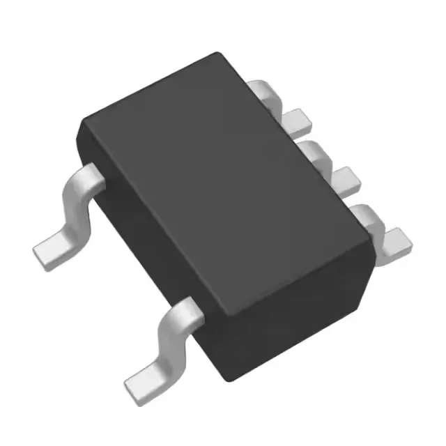
The SN74AUP1G08QDCKRQ1: For a BOM that already carries this order code, the supply channel is stable through authorized distribution and independent surplus. ROHS3 compliance is confirmed, so no regulatory conflict with EU or global automotive material declarations.
0.8V to 3.6V supply — the 74AUP family's low-voltage edge
The 0.8V minimum supply voltage lets this gate operate directly from a single lithium-ion cell near its end-of-discharge voltage — no boost converter needed for the logic rail. The 3.6V ceiling covers the full 3.3V nominal rail with margin for transients. At the 500 nA max quiescent current, the gate's own draw is negligible against the self-discharge rate of a coin cell or battery-backed module — an always-on sensor node or wake-up circuit won't drain the storage element through the logic. Propagation delay is 6.2 ns max at 3.3V into a 30 pF load — fast enough for the control logic in a 1 MHz SPI bus or a PWM enable path, but not intended for high-speed data lanes above 50 MHz where the output rise time into the load capacitance becomes the bottleneck.
The SC-70-5 (SOT-353) package footprint is 2.0 mm × 1.25 mm — small enough for the cramped PCB real estate inside an ECU module or a sensor housing where every square millimeter is budgeted.
4 mA output drive — standard CMOS fan-out, not a high-current buffer
The 4 mA source and sink capability at the output is typical for the 74AUP family — it drives up to four standard CMOS loads at 3.3V but won't directly switch an LED, a relay coil, or a long unterminated trace without a buffer stage. Input logic thresholds are 0.7V to 0.9V for low and 1.6V to 2V for high across the supply range — compatible with 1.8V and 2.5V logic families without external level translation, as long as the driving device's VOH exceeds the 1.6V threshold.