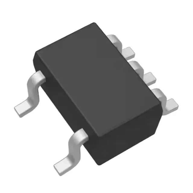
Single inverter with open-drain output for level translation and wired-OR buses
The SN74AUP1G06DCKR is a single inverter from Texas Instruments' 74AUP series, featuring an open-drain output that allows wired-OR connections and level translation between different voltage domains. Operating from 0.8V to 3.6V, it covers the full low-voltage logic range from sub-1V cores to 3.3V peripheral buses, with a typical quiescent current of just 500 nA.
Open-drain output — what it means for your bus topology
The open-drain output sinks 4 mA (low state) and floats high when off, so multiple outputs can share a common pull-up resistor to implement a wired-OR interrupt line or I²C-style bus without contention. Because the output does not source current, the high-level voltage is set by the pull-up rail — this lets the SN74AUP1G06DCKR translate a 1.8V input to a 3.3V output simply by tying the pull-up to 3.3V.
Propagation delay and signal integrity at 3.3V
Maximum propagation delay is 10.5 ns at 3.3V with a 30 pF load — fast enough for most GPIO-level handshakes and slow serial buses, but not intended for high-speed clock distribution. Input thresholds are 0.1V to 0.45V low and 3.6V high, meaning a 1.8V logic-high input is comfortably above the low threshold but may not reach the high threshold unless the supply is 1.8V or lower — check the input voltage against the supply rail.
Housed in a 5-lead SC-70-5 (SOT-353) package, the footprint is 2.0 mm × 2.1 mm with 0.65 mm pin pitch — a tight but hand-solderable layout that fits into space-constrained designs like sensor modules or wearable PCBs.
Lifecycle and compliance status
RoHS3 compliant (2011/65/EU + 2015/863), with no exemptions declared — suitable for EU-market products without additional substance declarations.