Active production — no end-of-life watch needed
The SN74AUP1G06DBVT: The 74AUP family remains a current catalog line for low-power logic designs. ROHS3 compliant, so no regulatory restriction on shipping into EU or UKCA markets.
Open-drain inverter — what the output stage buys you
This is a single inverter (one input, one output) with an open-drain (OD) output stage. The output can sink up to 4 mA but cannot source current — it pulls low when the input is high and goes high-impedance when the input is low. Open-drain lets you wire-AND multiple outputs onto a shared bus with a single pull-up resistor, or level-translate to a higher voltage rail by tying the pull-up to the target supply.
Quiescent current and propagation delay — the battery-life / speed trade-off
Maximum quiescent current is 500 nA across the full supply range and temperature. Propagation delay is 10.5 ns max at 3.3 V with a 30 pF load. That is fast enough for I2C bus buffering, enable/disable gating, or reset-line inversion at sub-MHz rates, but not for high-speed serial links above ~50 MHz — the open-drain output's rise time is set by the external pull-up resistor, not the IC itself.
SOT-23-5 footprint and temperature range
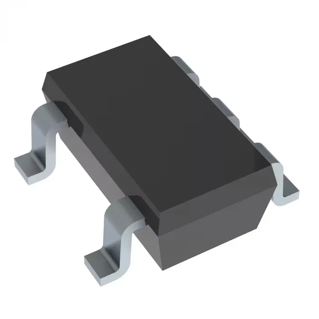
Housed in a 5-pin SOT-23 (SC-74A) package, the SN74AUP1G06DBVT occupies roughly 3 mm × 3 mm of board space. The pinout is standard for single-gate logic — VCC, GND, input, output, and a no-connect or optional enable pin depending on the variant.