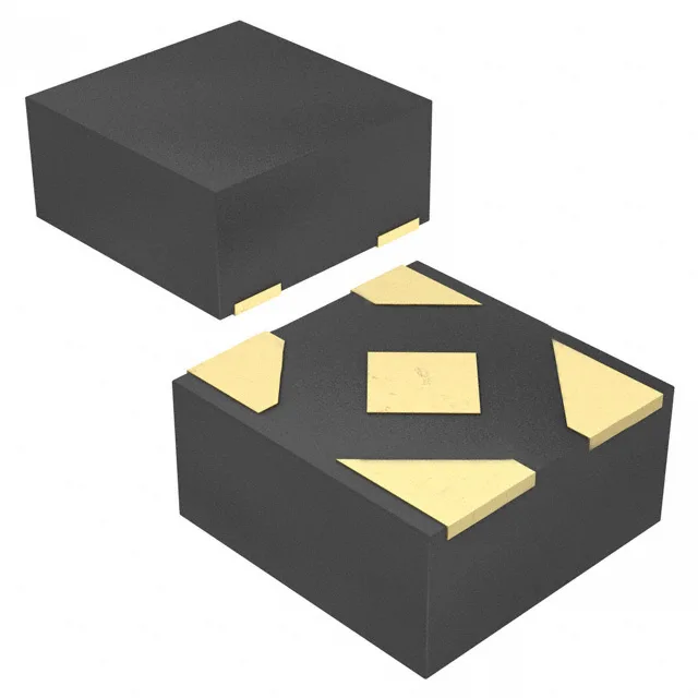
Single NOR gate for sub-1V to 3.6V rails
It operates from a supply range of 0.8V to 3.6V, making it suitable for battery-powered devices, IoT endpoints, and portable electronics where the core voltage may drop below 1V. The part draws a maximum quiescent current of 500 nA, which is critical for always-on sense circuits and wake-up logic. Output drive is rated at 4 mA for both high and low states, sufficient for driving light loads or interfacing to other low-power logic families.
6.4 ns propagation delay — timing budget for 3.3V buses
With a maximum propagation delay of 6.4 ns at 3.3V and 30 pF load, this gate fits into moderate-speed control and data paths. At lower supply voltages the delay increases, so for 1.2V or 0.8V operation the timing budget needs a wider margin. The 74AUP family is optimized for low dynamic power, and the 6.4 ns figure is typical for this process node — not a high-speed logic family, but adequate for GPIO expansion, interrupt routing, and enable/disable gating.
Package and footprint: 4-X2SON 0.8x0.8 mm
The SN74AUP1G02DPWR comes in a 4-XFDFN Exposed Pad package, also designated as the 4-X2SON with a 0.8x0.8 mm body. This is a very small, leadless package intended for space-constrained PCBs. The exposed pad provides a thermal path to the board — although for a 500 nA quiescent part, thermal dissipation is rarely a concern. The surface-mount footprint requires careful solder paste stencil design for the small pads.