Single NOR gate in the 74AUP ultra-low-power family
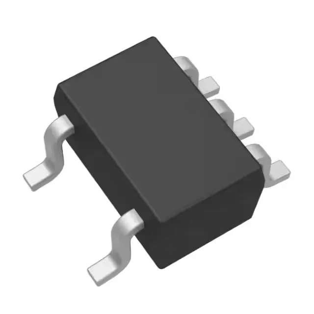
It operates from a 0.8V to 3.6V supply, making it suitable for battery-powered devices and multi-voltage systems without a separate level translator. The quiescent current maxes out at 500 nA, which keeps the idle draw negligible in always-on circuits like wake-up logic or sensor interfaces. Propagation delay is 6.4 ns at 3.3V with a 30 pF load, fast enough for most low-to-mid-speed digital buses but not meant for high-frequency clock trees. The SC-70-5 package (also known as SOT-353) is a 5-pin surface-mount footprint that saves board area but demands careful soldering — the 0.65 mm pitch is fine for reflow but tight for hand rework.
At 3.3V and 30 pF load, the max propagation delay is 6.4 ns. That is the worst-case number you need to budget in your timing analysis. If your system runs a 50 MHz clock (20 ns period), this gate eats about a third of the cycle — fine for combinatorial logic between registers, but too slow for critical-path gating in a 100 MHz+ design. At lower supply voltages the delay increases, so if you run at 1.8V expect roughly double the 3.3V figure. The 4 mA output drive is modest; if you are driving a long trace or multiple fan-outs, the extra capacitive load will stretch the delay beyond the datasheet limit.
500 nA quiescent — the battery-life decider
The 500 nA maximum quiescent current is the headline feature of the 74AUP family. That matters for always-on functions like power-on reset, interrupt combiner, or wake-up logic where the gate must stay powered continuously.
Package and footprint: SC-70-5
The SN74AUP1G02DCKR comes in an SC-70-5 package (also designated SOT-353), a 5-lead surface-mount package with 0.65 mm pitch and about 2.0 mm x 2.1 mm body. This is a space-saving footprint for dense boards, but the fine pitch means hand-soldering requires a fine-tip iron and steady hands — a hot-air rework station is easier.