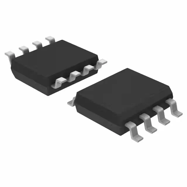
The two independent NAND circuits each sink or source 9 mA, enough to drive a light load or a single CMOS input on the same voltage rail. Propagation delay is 1.7 ns at 2.5V with a 30 pF load, fast enough for most serial interfaces and control signals in portable gear. The SM8 (SSOP) package is a small 8-lead footprint, surface-mount, and reworkable with standard hot-air tools — the 0.110-inch body width means you can get a tweezer tip under it without lifting adjacent passives.
Supply voltage and timing — the decision drivers
The 0.8V to 2.7V supply range is what defines this part: it is an ultra-low-voltage logic family. If your board runs on a 1.8V or 2.5V rail — common in modern MCU and FPGA designs — this gate works without a separate level translator. The input logic levels track the supply: low is 0V to 0.7V, high is 1.7V (at 2.5V supply). That 1.7V high threshold means it will not reliably see a 1.2V signal as a logic one; you need the supply at least that high. The 1.7 ns propagation delay at 2.5V is the headline speed — at lower supply voltages the delay increases, but the datasheet typical curve (not shown here) is consistent with the family. For a timing-critical path at 1.8V, budget roughly double that figure. The 10 µA quiescent current is negligible — the gate draws almost nothing when idle, which matters for always-on sensor nodes.
Not automotive-grade (no AEC-Q100), so skip it for under-hood or chassis-domain applications. The SM8 package is a standard SSOP-8 with a 2.80 mm body width. Reflow profile follows standard lead-free (ROHS3 compliant) with a peak around 260°C. No exposed pad, so no thermal-via stitching needed.
ROHS3 compliant, so no restriction on EU-market builds.