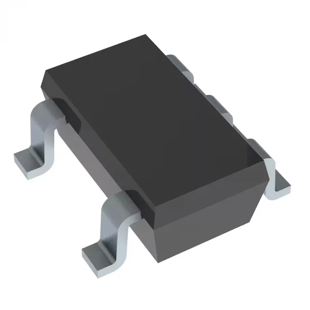
Texas Instruments SN74AUC1G08DBVR — Circuit Protection

SN74AUC1G08DBVR AND Gate, 0.8-2.7V, SOT-23-5

MPNSN74AUC1G08DBVR
End of Life

Texas Instruments 74AUC series AND Gate, SN74AUC1G08DBVR, single 2-input, 0.8V to 2.7V supply, 9mA output, SOT-23-5 package, Tape & Reel.

$0.49Ref. price · indicative, final on quote
PackagingSC-74A, SOT-753
StockContact for availability
Lead timeIn Stock wk
MOQ1 pcs
  • 100% new & originalTraceable channels only — no refurbs, no pulls, no remarked parts.
  • Date & lot codes on quoteStated per line before you commit; label photos on request.
  • MSL-compliant ESD packingMoisture-sealed bags with indicator cards; reels photo-verified.
  • PayPal buyer protectionPay by T/T, PayPal or Payoneer — card payments covered end to end.

Specifications

SN74AUC1G08DBVR Technical Specifications
ParameterValue
Series74AUC
Logic typeAND Gate
Mounting typeSurface Mount
Voltage0.8V ~ 2.7V
Current - quiescent10 µA
Current - output high, low9mA, 9mA
Number of inputs2
Operating temperature-40°C ~ 85°C
PackageTape & Reel (TR); Cut Tape (CT)
CaseSC-74A, SOT-753
Number of circuits1
Input logic level - low0.7V
Input logic level - high1.7V
Max propagation delay @ v, max CL2ns @ 2.5V, 30pF

Product details

Single AND gate for sub-3V logic rails

The SN74AUC1G08DBVR is a single 2-input AND gate from Texas Instruments' 74AUC series, designed for ultra-low-voltage operation from 0.8V to 2.7V. This makes it a natural fit for battery-powered or core-logic domains where the supply rail sits below 2.5V — think IoT endpoints, portable instruments, or SoC companion logic that must track a 1.2V or 1.8V bus.

Propagation delay and drive capability

Maximum propagation delay is 2ns at 2.5V with a 30pF load, so the gate keeps up with fast control signals in a 200+ MHz data path without adding a clock-cycle penalty. Output drive is symmetrical at 9mA source and sink — enough to switch a downstream flip-flop clock input or a small MOSFET gate through a series resistor, but not intended for heavy fan-out beyond four or five standard CMOS loads. Quiescent current maxes at 10 µA, meaning the gate's own draw is negligible in a sleep-mode budget — relevant when the AND function must remain powered to gate a wake-up signal while the rest of the system is off.

Package and footprint

Housed in the SOT-23-5 package (SC-74A body), the SN74AUC1G08DBVR occupies about 3mm² of board area. The 5-pin footprint is standard — no hidden thermal pad, no exposed paddle. It routes easily on a two-layer board; the 0.95mm pin pitch keeps the escape traces wide enough for 6-mil design rules without micro-vias.

Frequently asked questions

How do I get current pricing and availability for SN74AUC1G08DBVR?

Submit an RFQ through this listing. The SN74AUC1G08DBVR is sourced through independent distribution; current pricing and stock levels are confirmed at quote time.