Texas Instruments SN74AUC1G00DCKR — Discrete Semiconductors

SN74AUC1G00DCKR Texas Instruments NAND Gate, SC-70-5

MPNSN74AUC1G00DCKR
End of Life

Texas Instruments 74AUC series single 2-input NAND gate, SN74AUC1G00DCKR, SC-70-5 package, 0.8V to 2.7V supply, 9mA output drive, 2ns propagation delay.

$0.49Ref. price · indicative, final on quote
Packaging5-TSSOP, SC-70-5, SOT-353
RoHSROHS3 Compliant
Series74AUC
Independent supplier — new & surplus stockAuthenticity-screened · ESD-safe packingListing updated Aug 2026

Specifications

SN74AUC1G00DCKR specifications
ParameterValue
Series74AUC
Logic typeNAND Gate
MountingSurface Mount
Supply voltage0.8V ~ 2.7V
Current - quiescent10 µA
Current - output high, low9mA, 9mA
I/O channels2
Operating temperature-40°C ~ 85°C
PackageTape & Reel (TR); Cut Tape (CT)
Case5-TSSOP, SC-70-5, SOT-353
Number of circuits1
Input logic level - low0V ~ 0.7V
Input logic level - high1.7V
Max propagation delay @ v, max CL2ns @ 2.5V, 30pF

Product details

Single-gate NAND in the 74AUC family

The SN74AUC1G00DCKR is a single 2-input NAND gate from Texas Instruments' 74AUC series, a low-voltage logic family that operates from 0.8 V to 2.7 V. With a maximum quiescent current of 10 µA and propagation delay of 2 ns at 2.5 V into a 30 pF load, the part fits into high-speed, low-power signal paths where a single gate is needed without the overhead of a multi-gate package.

SC-70-5 footprint and board integration

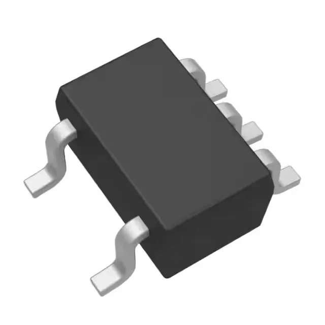
Housed in a 5-pin SC-70-5 (SOT-353) package, the SN74AUC1G00DCKR occupies roughly 2.0 mm × 2.1 mm of board area.

Supply voltage and logic-level thresholds

The 0.8 V to 2.7 V supply range covers the common 1.2 V and 1.8 V logic rails used in modern SoCs and FPGAs. The low-level input threshold accepts signals from 0 V to 0.7 V, while the high-level threshold is fixed at 1.7 V — meaning a 1.8 V CMOS output drives it cleanly, but a 1.2 V output may not reach the high threshold without a level shifter.

Output drive and switching speed

Symmetrical 9 mA source and sink drive at the output means the gate can switch capacitive loads like a single CMOS input or a short PCB trace without noticeable edge degradation. The 2 ns propagation delay at 2.5 V into 30 pF keeps the signal path clean for clock rates up to roughly 100 MHz in a point-to-point link.

Frequently asked questions

What is the SN74AUC1G00DCKR used for?

It is a single 2-input NAND gate from the 74AUC low-voltage logic family. It performs the NAND Boolean function on two inputs and outputs the inverted AND result. Typical uses include glue logic, signal gating, and level translation in circuits powered by 0.8 V to 2.7 V rails.

What package does SN74AUC1G00DCKR come in?

It is supplied in a 5-pin SC-70-5 (also known as SOT-353) surface-mount package.