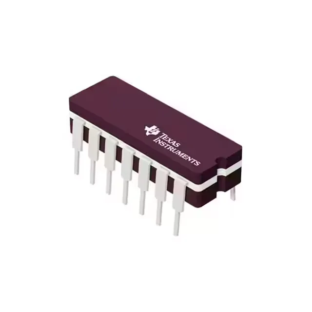
Texas Instruments SN74AS11N — Microcontrollers & Processors (MCU / MPU / DSP)

SN74AS11N 74AS Triple 3-Input AND Gate, 6ns @ 5V

MPNSN74AS11N
End of Life

Texas Instruments 74AS series SN74AS11N AND Gate, triple 3-input, 14-DIP (0.300", 7.62mm), through hole, 4.5V to 5.5V supply, 6ns propagation delay at 5V, 50pF.

$3.24Ref. price · indicative, final on quote
Packaging14-DIP (0.300", 7.62mm)
RoHSROHS3 Compliant
Series74AS
Independent supplier — new & surplus stockAuthenticity-screened · ESD-safe packingListing updated Aug 2026

Specifications

SN74AS11N specifications
ParameterValue
Series74AS
Logic typeAND Gate
MountingThrough Hole
Supply voltage4.5V ~ 5.5V
Current - quiescent7 mA
Current - output high, low2mA, 20mA
I/O channels3
Operating temperature0°C ~ 70°C
PackageTube
Case14-DIP (0.300\", 7.62mm)
Number of circuits3
Input logic level - low0.8V
Input logic level - high2V
Max propagation delay @ v, max CL6ns @ 5V, 50pF

Product details

6 ns propagation delay at 5 V, 50 pF

The SN74AS11N is a triple 3-input AND gate from the 74AS family, in a 14-pin DIP package. Its maximum propagation delay of 6 ns at 5 V with a 50 pF load sets the timing floor for the data path — at a 50 MHz clock, the gate delay consumes about 30% of a single clock period, leaving room for interconnect and setup margins.

Output drive and fan-out for TTL loads

The output stage sources 2 mA and sinks 20 mA — the asymmetric drive reflects the standard TTL totem-pole structure. The 20 mA sink capability drives up to ten standard LSTTL loads (each at 1.6 mA IIL), while the 2 mA source handles about five LSTTL loads (each at 0.4 mAIH). For a bus with mixed loads, the sink side is the limiting factor. Input logic thresholds are 0.8 V low and 2 V high, which are the classic TTL levels. A 0.8 V low threshold means the gate reliably interprets a 0.4 V LSTTL output as a logic low, but a 3.3 V CMOS output driving at 2.5 V may not reach the 2 V high threshold without a pull-up.

Active production, through-hole DIP

The 14-PDIP supplier package designation confirms the body width and pin spacing match the industry-standard DIP-14 layout.

Commercial temperature range, indoor use

Quiescent current draw is 7 mA max, which is typical for the AS (Advanced Schottky) process. In a 20-gate board, the total quiescent load is about 140 mA — well within a standard 5 V linear regulator's capacity, but worth budgeting in battery-powered designs.

Frequently asked questions

Will SN74AS11N drop into a board designed for SN74ALS11ANS?

No, the SN74ALS11ANS is a surface-mount SOIC package, while the SN74AS11N is a through-hole 14-DIP. The pin functions are the same (triple 3-input AND), but the footprints are incompatible without a board spin or an adapter. The ALS variant also has a slower 13 ns propagation delay at 5 V, 50 pF, versus 6 ns for the AS version.

What compliance documentation does Texas Instruments provide for SN74AS11N?

The SN74AS11N is RoHS3 compliant (EU RoHS exemption list through 2024). Standard TI documentation includes the datasheet, RoHS certificate of compliance, and material declaration. No UL or IEC certification is listed for this standard logic gate.