Logic function and timing margin
The SN74AS10N is a triple 3-input NAND gate from the 74AS family, packing three independent NAND circuits into a single 14-pin DIP. Each gate takes three inputs and outputs the NAND of those signals, a fundamental building block for glue logic, address decoding, or gating clock lines in a 5V digital system. Propagation delay is 4.5 ns typical at 5V with a 50 pF load, which sets the timing budget for a 5V bus running at tens of megahertz. The 2 mA source / 20 mA sink output drive handles standard TTL loads and short PCB traces without extra buffering.
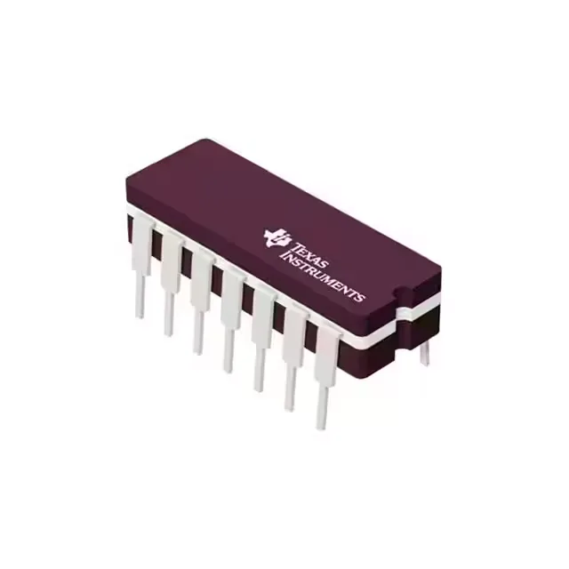
Housed in a 14-pin PDIP (0.300-inch body width), the SN74AS10N is a through-hole part that plugs into a standard 0.100-inch pitch socket or solders directly into plated-through holes. The wide 7.62 mm body gives good mechanical stability on a prototype board or production PCB, and the 0.300-inch row spacing is a common footprint shared by many 14-pin logic ICs. Input logic thresholds are 0.8V low and 2V high, compatible with standard 5V TTL and CMOS families that swing rail-to-rail.
It is not qualified for automotive or extended industrial ranges, so keep it inside a ventilated enclosure or rack.