Supply range, temperature grade, and propagation delay
The SN74AS04N: Maximum propagation delay is 5 ns at 5 V with a 50 pF load, which sets the timing budget for signal paths in synchronous designs. At 5 V, the 5 ns figure means the inverter can support clock rates up to roughly 100 MHz in a single-gate path, though the cumulative delay through six series stages must be budgeted in the overall timing closure.
Output drive and logic threshold margins
The output can source 2 mA and sink 20 mA, so it drives a single TTL load directly but cannot fan out to many CMOS inputs without a buffer. Input logic-low threshold is 0.8 V max and logic-high is 2 V min, providing standard TTL-compatible levels that interface cleanly with 5 V CMOS or older bipolar logic families.
Package and board integration
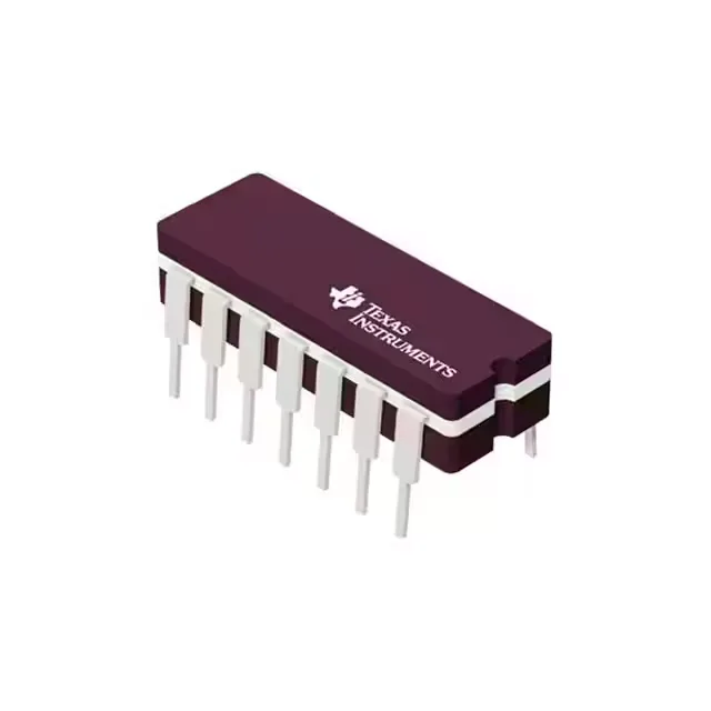
The 0.100-inch pin pitch and 7.62 mm row spacing are a legacy footprint that fits prototyping boards and production boards with no fine-pitch routing requirements.