150 MHz clock, 4.2 ns propagation delay — timing margin for 3.3 V buses
The SN74ALVCH16374DGVR is a dual 8-bit D-type flip-flop from the 74ALVCH family, clocked at 150 MHz with a maximum propagation delay of 4.2 ns at 3.3 V into a 50 pF load. That 4.2 ns window is the time the output takes to settle after the clock edge — at 150 MHz the clock period is 6.67 ns, so the output is valid for just over 2 ns before the next edge. For a shared address or data bus running at that speed, the setup and hold margins at the receiving end depend on this number, not the clock rate alone.
1.65 V to 3.6 V supply — mixed-voltage translation without a level shifter
The supply range spans 1.65 V to 3.6 V, so this flip-flop can sit on a 1.8 V core bus or a 3.3 V peripheral bus without a separate level translator. The input thresholds track the supply rail — at 1.8 V the VIH is about 1.2 V, which means a 1.8 V CMOS output drives it cleanly. The 24 mA output drive at both high and low is enough to fan out to four or five standard CMOS loads on a short trace, but at 3.3 V the edge rate into a long backplane trace will reflect — keep the stub length under an inch or add series termination.
Tri-state outputs and bus arbitration
The tri-state, non-inverted outputs let multiple flip-flops share a common data bus. When the output-enable pin is deasserted, the outputs go high-impedance and the bus floats — the next device on the line can drive it without contention. The 3 pF input capacitance per channel is low enough that eight flip-flops on a bus add only 24 pF of load, leaving headroom for the bus driver's capacitive drive limit.
Industrial temperature grade and surface-mount package
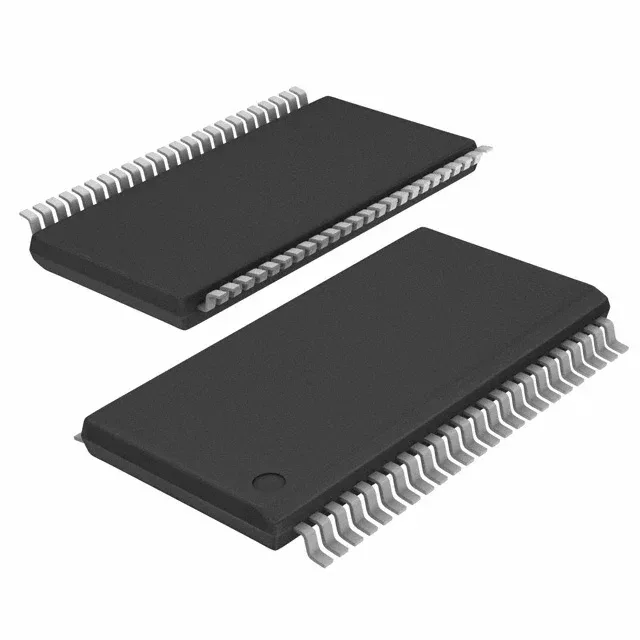
Rated for -40°C to +85°C ambient, the part covers factory-floor and outdoor cabinet environments without a commercial-temperature gap. The 48-TVSOP package is the thin version of TSSOP — 4.4 mm body width, 0.4 mm lead pitch. The footprint matches the standard TSSOP-48 land pattern, but the lower package height (1.2 mm max) matters if the board sits behind a cover with tight z-axis clearance. The quiescent current is 40 µA typical, so in a battery-backed system this flip-flop adds negligible draw when the clock is stopped.
Active lifecycle and sourcing posture
Texas Instruments lists the SN74ALVCH16374DGVR as Active with ROHS3 compliance. The part is sourced through authorized and independent distribution channels — quoted to order against the BOM quantity. For a BOM that already carries the 74ALVCH family, this flip-flop is a drop-in without a qualification cycle.