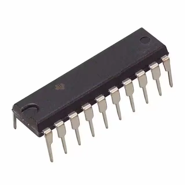
8-bit bus buffer with inverted tri-state outputs
The SN74ALS534AN is an octal D-type flip-flop from TI's 74ALS family — eight edge-triggered latches on a single die, clocked at 35 MHz, with tri-state inverted outputs. It sits on a 20-pin 0.300" PDIP and runs from a 4.5 V to 5.5 V rail. The inverted output polarity means the data bus sees the complement of the stored bit — useful when the downstream logic expects active-low signaling or when a bus transceiver's direction pin is already inverted.
Clock speed and output drive — timing margin in a legacy 5 V bus
Maximum clock frequency is 35 MHz, with a propagation delay of 16 ns at 5 V into a 50 pF load. That delay sets the setup/hold window for the downstream latch or register — budget it into your bus-cycle timing if the board already runs at 25-33 MHz. Output drive is asymmetrical: 2.6 mA source (high) and 24 mA sink (low). The sink current handles standard fan-out to 10 LSTTL loads; the weak source side means the rise time into a heavily loaded bus trace will be the limiting factor, not the propagation delay. Quiescent supply current is 19 mA typical — expect the full 8-bit bank to draw roughly that plus the switching current per output transition. Not a low-power part; plan the 5 V rail budget accordingly.
Package and temperature — through-hole board fit
Housed in a 20-lead PDIP (0.300" body width, 7.62 mm), the SN74ALS534AN is a through-hole part. No reflow profile needed — wave-solder or hand-solder into a plated through-hole board. The 0.100" pitch matches standard prototype grid and legacy backplane layouts. Rated for commercial temperature range: 0°C to 70°C ambient. Not specified for industrial or automotive environments — keep it in conditioned indoor equipment or lab gear.
Sourcing and availability — quoted per BOM line
Sourced through authorized and independent distribution channels on a per-RFQ basis. Current pricing and lead time are confirmed at quote time against your BOM quantity. Tube packaging — 20 units per tube typical for PDIP.