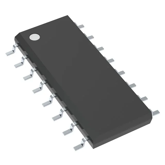
Texas Instruments SN74ALS259D — Logic ICs

SN74ALS259D 8-Bit Addressable Latch, 2 ns Propagation Delay

MPNSN74ALS259D
End of Life

Texas Instruments 74ALS series SN74ALS259D, 8-bit D-Type Addressable Latch, 1:8 circuit, 2 ns propagation delay, 4.5 V to 5.5 V supply, 400 µA / 8 mA output drive, 0°C to 70°C, 16-SOIC surface mount package.

$4.03Ref. price · indicative, final on quote
Packaging16-SOIC (0.154", 3.90mm Width)
RoHSROHS3 Compliant
Series74ALS
Independent supplier — new & surplus stockAuthenticity-screened · ESD-safe packingListing updated Aug 2026

Specifications

SN74ALS259D specifications
ParameterValue
Series74ALS
Logic typeD-Type, Addressable
Output typeStandard
MountingSurface Mount
Voltage4.5V ~ 5.5V
Current - output high, low400µA, 8mA
Operating temperature0°C ~ 70°C
Circuit1:8
PackageTube
Case16-SOIC (0.154\", 3.90mm Width)
Independent circuits1
Delay time - propagation2ns

Product details

Its headline rating is a 2 ns propagation delay, placing it in the fast end of the 5 V TTL logic spectrum for address decoding, register file expansion, or demultiplexing applications. The 1:8 circuit topology means a single data input fans out to eight individually addressable storage latches, each with a standard TTL output that sinks 8 mA and sources 400 µA.

Output drive — fan-out and CMOS interface

The 400 µA high-level output current and 8 mA low-level output current are typical of standard ALS TTL. Driving a CMOS load with high-impedance inputs is fine, but if the downstream logic is 5 V CMOS with 1 µA input leakage, the fan-out is limited by the capacitive load and edge rate, not the DC current. For bus-oriented designs with multiple loads, the 8 mA sink handles up to 10 standard ALS inputs per the family fan-out rules.

Dual role: addressable latch and 1-of-8 demultiplexer

The addressable latch architecture allows the SN74ALS259D to function as either an 8-bit storage register or a 1-of-8 demultiplexer, depending on the control pin strapping. When the latch-enable is held active, the address lines select which output follows the data input — a demultiplexer. When the data input is held static and the latch-enable strobes, the addressed bit stores the data. This dual role saves a separate decoder IC in address-mapped I/O or status-register bank designs.

Package and footprint — 16-SOIC surface mount

The surface-mount form factor suits automated assembly for medium-density PCBs. No exposed thermal pad — junction-to-ambient thermal resistance is handled through the SOIC leads and copper trace area.

Frequently asked questions

What is the difference between SN74ALS259 and SN74ALS259D?

The suffix 'D' indicates the surface-mount 16-SOIC package. The base SN74ALS259 is the through-hole DIP variant.

Can SN74ALS259D be used as a demultiplexer?

Yes. With the latch-enable held active, the address lines select which of the eight outputs follows the data input, implementing a 1-of-8 demultiplexer. This is a documented operating mode of the addressable latch architecture.

When sourcing SN74ALS259D, what is the closest functional second-source — 74FCT573APC?

The 74FCT573APC is a different logic function — it is an 8-bit transparent latch (8:8), not an addressable latch (1:8). The 74FCT573APC has an 8.5 ns propagation delay and 15 mA output drive, but it lacks the addressable/demultiplexer capability. For a direct functional equivalent, stay within the 74ALS259 family; the 74FCT573APC is not a pin-compatible or functional substitute.