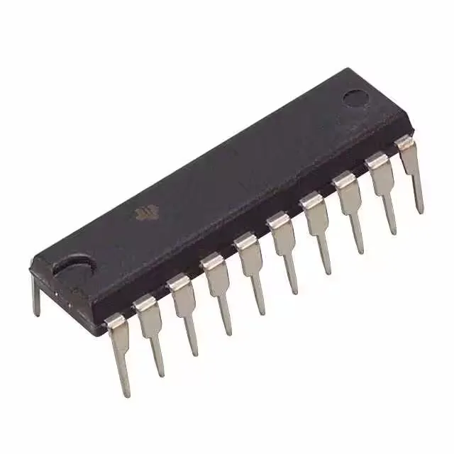
8-bit edge-capture with 115 MHz clock ceiling
The SN74AHCT574N: The propagation delay is 10.6 ns max at 5 V into 50 pF — this sets the data-to-output settling window for bus-margin analysis; the clock-to-Q time must fit within the downstream setup-hold budget of the receiving device. Outputs are tri-state and non-inverted, so the part can be ganged on a shared data bus without contention — the output-enable control (OE) pulls the bus into high-Z when inactive.
Supply, temperature, and standby profile
The industrial temperature grade spans -40°C to 125°C, covering most factory-floor and outdoor telecom enclosures without derating. Quiescent current is 4 µA typical — negligible for an always-powered bus-hold or address-latch application. The input capacitance is 3 pF per pin, which keeps the clock-line loading low when multiple devices share a common clock tree.
Through-hole package and board-fit
The supplier device package is 20-PDIP; the body width is 0.300 inch, so it fits the narrower DIP footprint, not the 0.600-inch wide-body. For a board rework or repair scenario, the through-hole package is easier to desolder than a fine-pitch SMD.
The 74AHCT series is a 5 V CMOS logic family with TTL-compatible input thresholds.