Clock edge and propagation timing
The SN74AHCT174D is a single-element D-type flip-flop with master reset, clocked on the positive edge. Six bits per element, non-inverted outputs. The maximum clock frequency of 115 MHz sets the upper data rate the flip-flop can sustain — above that the setup-and-hold window at the D input closes, and the output no longer tracks the clock edge reliably. Propagation delay is 8.8 ns max at 5 V supply into a 50 pF load. That delay is the time from the clock edge to valid Q output; it adds directly to the timing budget of the downstream logic. With 8 mA symmetric output drive (both high and low), the rise and fall times into the load capacitance are well-controlled, but the 8.8 ns figure already includes that transition.
Supply rails and temperature range
The 74AHCT family is TTL-compatible at the input thresholds, so it interfaces directly with 5 V TTL logic without a level shifter. Quiescent current is 4 µA typical, negligible in a powered system. This covers most factory-floor, outdoor telecom, and automotive cabin environments; the part is not qualified for extended -55 °C or 125 °C military/under-hood use. Input capacitance is 2 pF per pin, which loads the driving gate minimally.
Package, compliance, and sourcing
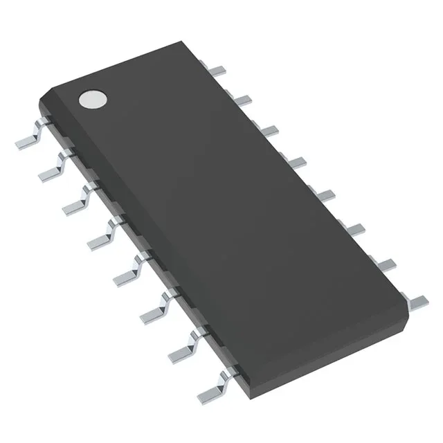
The narrow-body SOIC footprint is common and routes well on two-layer boards. Supplied in Tube packaging. ROHS3 compliant per the lifecycle record. No PCN or EOL notice on file.