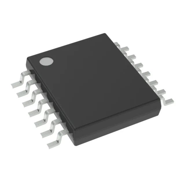
Quad 2-input NAND gate for 5V TTL systems
The SN74AHCT00PWR from Texas Instruments is a quad 2-input NAND gate from the 74AHCT series, designed for 5V TTL-compatible logic systems. It integrates four independent NAND gates in a single 14-TSSOP package, each with two inputs, making it a compact building block for glue logic, signal gating, and combinatorial functions on mixed-voltage boards. Operating from a 4.5V to 5.5V supply, the device accepts TTL input levels: a low threshold of 0.8V and a high threshold of 2V. This ensures direct interfacing with 5V TTL outputs without external level translation, simplifying BOM integration in legacy or mixed-logic designs.
Propagation delay and output drive
Maximum propagation delay is 7.9ns at 5V with a 50pF load, which sets the timing budget for the signal path. For a 5V system clocked at 50 MHz, this delay represents less than half a clock period, leaving margin for trace delays and input capacitance from downstream loads. The symmetrical drive current simplifies fan-out calculations — the same 8mA figure applies for both high and low states, so the output rise and fall times remain balanced across the load range.
Temperature range and quiescent current
The 2 µA maximum quiescent current keeps the power budget negligible in battery-backed or always-on subsystems.
Supplied in a 14-TSSOP package with 0.173-inch body width and 4.40mm height, the device occupies a compact footprint on the PCB.