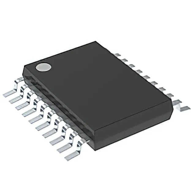
Package and board integration
The SN74AHC374PWR comes in a 20-TSSOP package (4.40 mm width, 0.65 mm pin pitch). This is a standard fine-pitch surface-mount footprint that routes cleanly on a two-layer board if the supply decoupling caps sit within 5 mm of the VCC/GND pins. The 0.65 mm pitch means the PCB land pattern follows the IPC-7351A SOT360-1 recommendation — no via-in-pad needed, but the solder paste stencil aperture should be 1:1 with the pad to avoid bridging on the inner rows.
Supply voltage and timing margin
The 2 V to 5.5 V supply range covers 3.3 V and 5 V logic rails without a separate level translator on the input side. At 5 V the propagation delay is 6.9 ns max into a 50 pF load — this sets the data setup time budget for the downstream latch or bus receiver. The 120 MHz clock frequency ceiling means the part handles 8-bit parallel data transfers at 120 million words per second. The positive-edge trigger synchronises the data capture to the rising clock edge, which simplifies timing closure in a single-clock-domain design. Quiescent current is 4 µA typical — negligible in a powered system, but relevant if the flip-flop sits in a battery-backed register bank where the supply stays on during sleep.
Output drive and bus architecture
The tri-state, non-inverted outputs source or sink 8 mA per pin. This is enough to drive a single TTL/CMOS load or a short (< 30 pF) bus trace directly. For heavily loaded backplanes or long parallel buses, a buffer after the output is recommended to keep the rise time within the next stage's input threshold window. With eight bits per element in a single package, the SN74AHC374PWR maps cleanly to an 8-bit data register or address latch. The tri-state control lets multiple devices share a common data bus without contention.
Temperature grade and environment
Rated for -40°C to +85°C ambient (TA), this is the industrial temperature range. The part is suitable for factory-floor controllers, telecom cabinets, and outdoor equipment enclosures that see diurnal temperature swings. Input capacitance is 4 pF per pin — the capacitive load on the driving stage is low, which helps maintain signal integrity on the clock and data lines at 120 MHz.
Lifecycle and compliance
The 74AHC series is a mature 5 V CMOS logic family. The SN74AHC374PWR is a standard catalogue part — no allocation risk or single-source dependency flagged in the supply chain data.