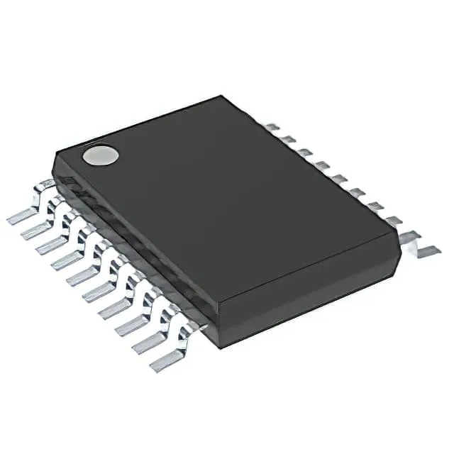
The SN74AHC245QWRKSRQ1 comes in a 20-VFQFN exposed pad package (2.5x4.5 mm body) with wettable flank terminals — the side-plating allows automated optical inspection (AOI) of the solder fillet after reflow, which is a requirement for automotive-grade assembly lines where hidden solder joints under the package are not acceptable.
Drive strength and bus architecture
Each of the eight channels sources or sinks 8 mA (at VCC = 4.5 V) — enough to drive a 50 pF bus load at 10 MHz with clean edges, but the 3-state outputs let multiple transceivers share a common data bus without contention when the output enable is deasserted. The non-inverting transceiver architecture means data flows from A to B (or B to A) with the same logic polarity — no inversion to account for in the firmware or FPGA logic.
ROHS3 compliant — no exemptions for lead in solder, so it passes the EU RoHS directive without a certificate-of-exemption chase.