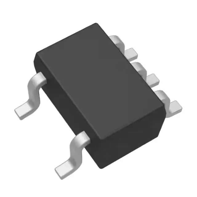
Automotive-grade OR gate in a 5-pin SC-70
The SN74AHC1G32TDCKRQ1: Housed in a 5-pin SC-70-5 (SOT-353) package, it occupies minimal board area — roughly 2.0 mm × 2.1 mm — making it suitable for space-constrained ECU modules or sensor interface boards where a single glue-logic gate is needed. Input logic levels are specified as 0.5 V to 1.65 V for low and 1.5 V to 3.85 V for high, giving it TTL-compatible thresholds that reject noise on slow-rising signals from switches or sensors.
Propagation delay and output drive for timing closure
Maximum propagation delay is 7.5 ns at 5 V with a 50 pF load. This sets the timing budget for the logic path — if the downstream flip-flop has a 2 ns setup time, the OR gate plus interconnect must deliver the signal within 5.5 ns of the clock edge for a single-cycle path. At lower supply voltages the delay increases; at 3.3 V it typically runs about 10 ns. Symmetric output drive of 8 mA source and sink at 5 V means the gate can drive moderate capacitive loads or fan out to four or five standard CMOS inputs without buffering. The quiescent current is just 1 µA maximum, so in a key-off automotive module the gate's own draw is negligible against the system sleep budget.
Temperature range and deployment in automotive systems
For designs targeting 125°C ambient, the SN74AHC1G00DBVT (NAND gate, same family) is rated to 125°C. ROHS3 compliant and free of the six restricted substances plus four phthalates, so it meets the material declarations for automotive OEMs that require full REACH compliance documentation.
Sourcing and lifecycle position
The closest functional peer is the SN74AHC1G32DCKT — same logic function, same 2-input OR gate, same 74AHC family. The package is identical SC-70-5, so a board designed for one accepts the other without layout changes. If your application stays below 85°C, the DCKT is a cost-optimized drop-in.