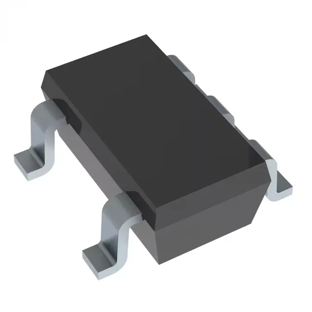
Single AND gate in a SOT-23-5 — open-drain output for wired-OR buses
The SN74AHC1G09DBVR is a single 2-input AND gate from Texas Instruments' 74AHC series, packaged in a 5-pin SOT-23-5 (SC-74A) footprint. The distinguishing feature is the open-drain output — the high-side driver is absent, so the output can only sink current to ground, not source it. This makes the part a natural fit for wired-OR or active-low bus structures where multiple gate outputs share a common pull-up resistor. The input logic thresholds scale with VCC: low-level threshold is 0.5V to 1.65V, high-level is 1.5V to 3.85V, so it interprets standard CMOS and TTL levels correctly across the range.
Open-drain output — what the 8mA sink rating means on the bench
The output stage is specified as '-, 8mA' — the dash means no high-level output current is specified because the open-drain FET only pulls low. The 8mA figure is the maximum sink current the low-side FET can handle while staying within the output voltage spec (typically VOL ≤ 0.5V at rated current). For a pull-up resistor calculation: at 5V supply with a 1kΩ pull-up, the sink current is 5mA — well within the 8mA limit, and the VOL will be under 0.3V. Propagation delay is 7.5ns max at 5V with a 50pF load — this is the time from input crossing the threshold to the output falling below VOL. The open-drain output's rise time is set entirely by the external pull-up resistor and load capacitance, not by the gate itself. For high-speed lines, keep the pull-up value low enough to charge the bus capacitance within the required cycle time. Quiescent current is 1µA maximum across the full temperature range. In battery-powered or always-on circuits, this gate adds negligible standby drain — the pull-up resistor's leakage path typically dominates the idle current budget.
Active production — sourcing and compliance
The ROHS3 compliance means the part is free of the ten restricted substances including lead, mercury, and cadmium — no exemption expiry to track. The part carries the standard TI datasheet with electrical characteristics, switching waveforms, and application notes for wired-OR bus design.