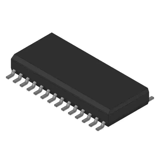
512 x 9 asynchronous FIFO in 28-SOIC
The Texas Instruments SN74ACT7201LA25DVR is a 4.5 Kbit (512 x 9) asynchronous FIFO memory in a 28-SOIC surface-mount package. As an asynchronous FIFO, it uses independent read and write control signals rather than a shared clock — the 25 ns access time sets the minimum read-cycle period, and the 28.5 MHz data rate defines the maximum write throughput. This makes it a fit for bridging data between two asynchronous clock domains where the latency budget is tight.
25 ns access time and retransmit capability
The 25 ns access time is the time from the read-enable edge to valid data on the output bus — in a system where the downstream logic samples on the same edge, this sets the setup-time margin at the receiver. The 28.5 MHz data rate corresponds to a 35 ns write-cycle period, so the FIFO can accept a new word every 35 ns on the write side. Retransmit capability allows the read pointer to be reset to the first unread word without clearing the entire FIFO — useful when a data packet must be re-read after a CRC error. The device also supports depth and width expansion, so multiple parts can be cascaded for deeper or wider buffers without external logic. Maximum supply current is 125 mA — this is the total current drawn from the 5 V rail under worst-case conditions. The 512 x 9 organization stores nine bits per word, so the ninth bit can serve as a parity or tag bit alongside the eight data bits.
Active lifecycle and 28-SOIC board integration
The 28-SOIC package has a standard 1.27 mm pitch and 300-mil body width — a common footprint that routes easily on two-layer boards.