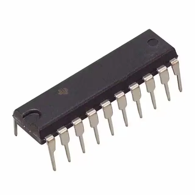
Through-hole 8-bit register with inverted bus drive
The SN74ACT564N is an 8-bit D-type flip-flop from the 74ACT family, clocked on the positive edge and delivering inverted, tri-state outputs. It is a standard-function register — no set or reset pins — intended for bus-oriented storage where the output polarity is inverted relative to the data input. Housed in a 20-pin DIP (0.300" body width, 7.62 mm row spacing), it is a through-hole part for boards where wave solder or hand assembly is preferred over reflow. The 20-PDIP footprint is a legacy standard — still common in industrial control, test equipment, and retrofit designs that avoid surface-mount rework.
Clock speed and propagation delay — the timing budget
Rated for a 90 MHz maximum clock frequency, this flip-flop can capture data at a 90 MHz toggle rate — fast enough for most parallel bus interfaces in 5 V systems. The propagation delay is 10.5 ns max at 5 V into a 50 pF load, which sets the data-to-output settling time after the clock edge. That 10.5 ns window must fit within the bus cycle timing; if the downstream latch setup time plus trace delay exceeds the clock period minus 10.5 ns, the data will not be valid on time. The 24 mA output drive (both source and sink) gives enough current to drive a heavily loaded bus or a bank of LEDs directly, but the 4 µA quiescent current is negligible for power budgeting.
Temperature grade and compliance
Texas Instruments lists this part as Active in production and ROHS3 Compliant.