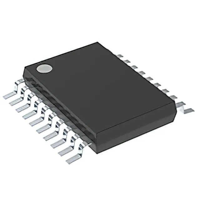
The SN74AC574PWR comes in a 20-TSSOP package (4.40 mm width, 0.65 mm pitch) — a hand-solderable footprint if you have a fine tip and steady hands, though a hot-air station makes it easier. The 0.65 mm pitch is forgiving enough for a two-layer prototype board with careful trace routing. Surface-mount only — no through-hole variant in this series. The 20-TSSOP supplier device package is the same as the package/case, so the footprint is consistent across the TI 74AC octal D-type line.
Clock speed and timing margin
Rated for 153 MHz clock frequency — that is the maximum toggle rate for the flip-flop itself. The real throughput in a bus application depends on the propagation delay and the output loading. Max propagation delay is 9.5 ns at 5 V supply with a 50 pF load. That means the data at the output is valid 9.5 ns after the clock edge — budget this into your setup/hold timing analysis, especially if the downstream device has tight hold requirements. The 24 mA output drive (both high and low) gives you enough current to drive a 50 pF bus trace or a short ribbon cable without external buffers. For longer runs or higher fan-out, the rise time will degrade — keep the trace length under 6 inches at 153 MHz.
Supply voltage and temperature envelope
Operates from 2 V to 6 V — this is the full 74AC supply range. At 3.3 V it runs fine; at 5 V it hits the rated 153 MHz. The 4 µA quiescent current is negligible for battery-powered designs that spend most of their time in standby. This covers most factory-floor and outdoor telecom enclosures.
RoHS3 compliant (2011/65/EU + 2015/863). No REACH or UL documentation is on the record, but TI typically provides REACH declarations on request.