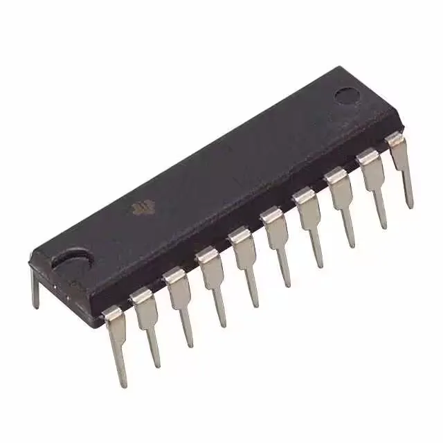
153 MHz clock ceiling for bus-register timing
The SN74AC574N: The 9.5 ns propagation delay at 5 V, 50 pF load means the data must be stable at the D inputs well before the positive edge — the setup-time window shrinks as the clock rate approaches the 153 MHz ceiling.
24 mA drive and tri-state bus control
Each of the eight outputs sources or sinks 24 mA — enough to drive a parallel bus line or a bank of LEDs without a buffer. The tri-state, non-inverted outputs let multiple devices share a data bus; the output-enable control pulls all outputs to high-impedance, which is the standard pattern for a registered transceiver or address latch on a processor bus. Quiescent current is 4 µA typical, so in a battery-backed panel the part draws negligible standby power when the clock is gated off.
Industrial temperature and through-hole package
The 20-pin DIP (0.300-inch width) with 0.100-inch pitch is a standard through-hole footprint — it sockets into a legacy board or a prototyping breadboard without a carrier. Input capacitance is 4.5 pF per pin, which keeps the bus loading manageable when multiple flip-flops are daisy-chained on the same clock line. The positive-edge trigger type matches the majority of synchronous bus protocols; no inversion on the outputs simplifies the logic trace.
Active production — sourcing and compliance
Supplied in tube packaging, the 20-DIP body is the same footprint used for decades — the date-code laser etch on the top side and the tube label should trace back to TI's assembly site for that week.