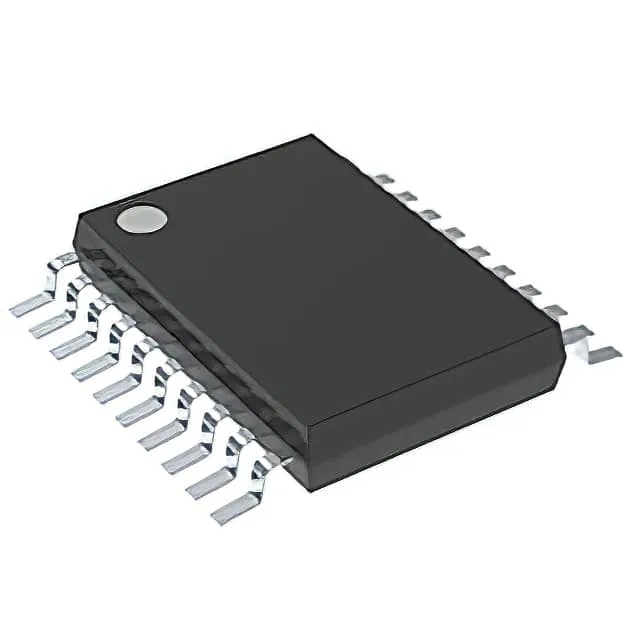
20-TSSOP footprint and board-level integration
The SN74AC563PW: The supplier device package is 20-TSSOP, so the PCB footprint matches the standard JEDEC MO-153 variation; no custom pad geometry is needed.
Bus drive and timing margin for 8-bit data paths
The 4.6 ns propagation delay (VCC = 5 V, CL = 50 pF) sets the data-valid window for an 8-bit address or data latch — at a 50 MHz bus clock (20 ns period), the latch has 15.4 ns of setup-and-hold margin after the clock edge, which comfortably accommodates PCB trace skew under 2 ns. Output drive is rated 24 mA source and 24 mA sink — this is enough to drive a 50 pF bus load at 50 MHz without external buffers, but the total simultaneous-switching output current must stay within the package's thermal limit (not explicitly derated here; the 24 mA figure is per-pin, not summed). The tri-state outputs (active-low output-enable pin) let multiple latches share a common data bus without contention — the high-impedance state leakage is low enough that 8 devices on the same bus add less than 1 µA of off-state current.