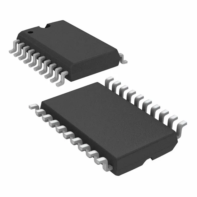
24-SOIC footprint and 125 MHz clock — what the ratings mean for the bus
The SN74ABT821ADW is a single-element 10-bit D-type flip-flop from the 74ABT family, clocked at 125 MHz with a positive-edge trigger. It stores and forwards a 10-bit wide data word on each rising clock edge, making it a fit for address/data latching in a 5 V bus interface. The 6.2 ns max propagation delay at 5 V and 50 pF load sets the timing budget for the downstream logic — at 125 MHz the clock period is 8 ns, so the output settles within 77.5% of the cycle, leaving about 1.8 ns of hold margin before the next edge. That is tight; the board trace length and load capacitance need to stay within the datasheet's derating curve. Tri-state non-inverted outputs with 32 mA source / 64 mA sink drive let the part directly control a 5 V backplane or a bank of LEDs without a buffer — the 64 mA sink handles the transient inrush of a heavily loaded bus line. The 3.5 pF input capacitance per channel keeps the clock-line loading low enough that a single 125 MHz source can fan out to several devices without a dedicated clock buffer.
The 250 µA quiescent current is negligible in a powered system — the dynamic draw at 125 MHz will dominate the power budget, but the standby current is low enough that a shared 5 V rail serving multiple logic devices won't see a meaningful idle load from this flip-flop.