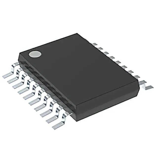
20-TSSOP footprint and 200 MHz clock ceiling
The SN74ABT574APWR is an 8-bit D-type flip-flop in a 20-TSSOP package (4.40 mm width, 0.173" body), positive-edge triggered with tri-state non-inverted outputs. It belongs to the 74ABT family, TI's advanced BiCMOS logic series that balances speed against static power for 5 V bus applications. The 200 MHz clock frequency is the toggle rate ceiling — at that edge rate the propagation delay of 6.6 ns max at 5 V into 50 pF sets the data-to-output timing budget. For a pipeline register clocked at 150 MHz, the 6.6 ns tpd leaves roughly 0.7 ns of setup margin before the next edge, assuming a 50% duty cycle clock.
Output drive and supply rail
Output drive is rated 32 mA source and 64 mA sink — this is enough to directly drive a 50 Ω backplane trace or a bank of LED indicators without a buffer. The 4.5 V to 5.5 V supply range means it runs on a nominal 5 V rail with ±10% tolerance, covering the full ATX or industrial 5 V bus. Quiescent current is 250 µA typical — the BiCMOS output stage draws minimal static current when the outputs are static, but the dynamic current scales with clock frequency and load capacitance. At 200 MHz with all eight outputs switching into 50 pF each, the dynamic current adds roughly 80 mA, so the total supply draw is dominated by the switching load, not the 250 µA Iq.
Temperature grade and input capacitance
Rated for -40°C to 85°C ambient — this is the industrial temperature band. The 3.5 pF input capacitance per pin means the clock line sees about 28 pF total when all eight data inputs are driven in parallel, which is within the drive capability of most 5 V CMOS or TTL clock sources without a dedicated buffer. The 6.6 ns propagation delay is specified at 5 V supply into a 50 pF load — the worst-case delay at the minimum supply voltage (4.5 V) will be slightly higher, so for timing closure at 4.5 V the designer should budget an additional 1-2 ns of margin.