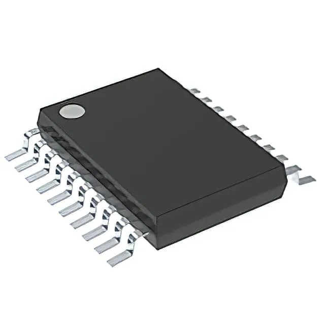
8-bit D-type in 20-TSSOP — clock edge and output drive
The SN74ABT574APW: That delay sets the timing margin for the data-to-output path — at 200 MHz the clock period is 5 ns, so the 6.6 ns propagation means this part is not a full-cycle pipeline register at that frequency; it is best used where the clock-to-output timing is absorbed into the downstream setup window. Output drive is 32 mA source, 64 mA sink — enough to drive a 50 Ω backplane or a bank of LED indicators without a buffer. The tri-state control lets multiple outputs share a common bus; the high-impedance state is active when the output-enable pin is deasserted.
Supply rails and temperature grade
Quiescent current is 250 µA typical, so the static power draw is negligible in a 5 V system. This covers most factory-floor and outdoor enclosure environments, but not extended automotive under-hood ranges. Input capacitance is 3.5 pF per pin — light enough that a 50 Ω source can drive eight parallel inputs without excessive signal degradation at 200 MHz.