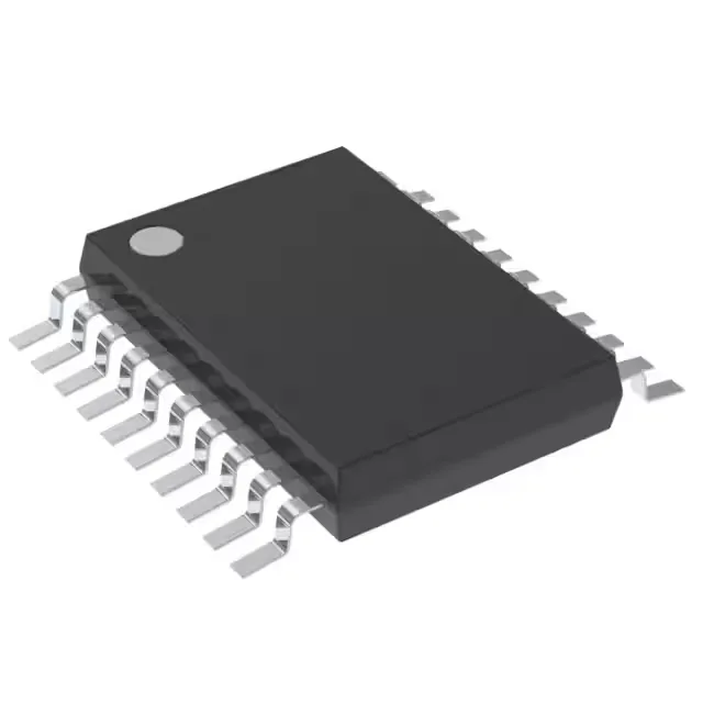
200 MHz clock and 6.6 ns propagation delay
The SN74ABT574ANSR: The 200 MHz clock sets the data rate ceiling for the bus; the 6.6 ns delay means the output settles within one clock cycle at that speed, leaving timing margin for the downstream logic. Output drive is 32 mA sink and 64 mA source, enough to drive a heavily loaded data bus or multiple fan-out loads without needing a buffer. Quiescent current sits at 250 µA, so the part's own draw is negligible in a mixed-signal supply budget.
Supplier device package is 20-SO.
Supply voltage and input capacitance
Input capacitance is 3.5 pF per pin, light enough that a single 5 V CMOS driver can clock several of these flip-flops without signal degradation from capacitive loading. The positive-edge trigger and tri-state non-inverted outputs make it a direct fit for registered data buses where the outputs share a common bus line and need to be disabled during read cycles.