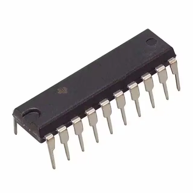
This is a standard catalog item, not a last-time-buy or NRND part. For BOM planning, the 20-DIP through-hole package is widely stocked across distribution channels, so lead times tend to be stable — no special procurement gymnastics needed to qualify it into a production line.
Output drive and bus loading — what the 32mA/64mA rating means
The 32mA source / 64mA sink capability is the headline selection parameter for this buffer. It determines how many standard TTL loads the output can fan out to without signal degradation. At 5V, each output can drive up to 10 LSTTL loads or about 30 CMOS loads (assuming 10pF per input). If your bus has more than 8 loads per line, or if the trace length exceeds 6 inches, plan for a series damping resistor (22-33Ω) to control overshoot. The 3-state outputs let multiple buffers share a bus without contention — the output enable control is active-low per the 74ABT541 function table.
Package and assembly — through-hole DIP considerations
The 20-DIP (0.300" body width, 7.62mm lead pitch) is a legacy through-hole package. It requires a 0.100" row-to-row spacing on the PCB. If your assembly line is wave-solder only, this part drops in without reflow profile changes. For hand-prototype or rework, the DIP is easier to socket than SOIC. Note that the 74ABT series has faster edge rates than older 74LS/74HC families — the fast switching can cause ground bounce if the supply decoupling is weak. Place a 0.1µF ceramic cap within 0.5" of each VCC pin.