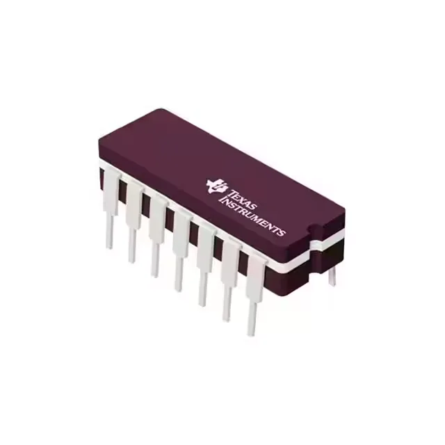
Texas Instruments SN7404N — Analog & Data Acquisition
Technical Documents PDF / CAD
RoHS Compliant · Lead-Free EIA-481 Standard
Texas Instruments / Analog & Data Acquisition

Texas Instruments SN7404N Hex Inverter, 14-DIP, 4.75-5.25V

MPN SN7404N
End of Life Spot Stock · 24-48h Dispatch 100% Original Sealed

Texas Instruments 7400 series hex inverter, SN7404N, 6-circuit, 14-DIP through-hole package, 4.75-5.25V supply, 22ns propagation delay at 5V/15pF.

In Stock: 13 pcs
MOQ: 1 pcs
Logistics: DHL / FedEx DAP (Global Express · 3-7d) Russia & CIS DDP (Door-to-Door Cleared)
Dispatch: Shenzhen / HK
Unit Price (USD)
$4.07 / pc
Direct Purchase Ready
Volume Pricing Breaks Confirmed upon quotation
1+ pcs
$4.07
10+ pcs
$3.48
Working on a production BOM or have a target unit price? Submit Target Price
Buy Now

$4.07 / ea

13 in stock — maximum per order · 3–4 days lead time

$3.48 / ea from 10 pcs

Upload Full BOM List
[SPEC] Essential Parameters Snapshot Full Specifications (13)
Package / Case 14-DIP (0.300", 7.62mm)
Supply Voltage 4.75V ~ 5.25V
Output / Current 400µA, 16mA

Full Technical Specifications

13 Parameters
SN7404N specifications
Parameter / AttributeSpecification / Value
Series7400
Logic typeInverter
MountingThrough Hole
Supply voltage4.75V ~ 5.25V
Current - output high, low400µA, 16mA
I/O channels1
Operating temperature0°C ~ 70°C
PackageTube
Case14-DIP (0.300\", 7.62mm)
Number of circuits6
Input logic level - low0.8V
Input logic level - high2V
Max propagation delay @ v, max CL22ns @ 5V, 15pF
Series Sibling Variants

Texas Instruments 7400 Series Models

Sibling variants, package options, and speed/density grades in this Texas Instruments semiconductor series. Active Shenzhen warehouse allocation and rapid 24-48h dispatch.

Technical Details & Description

Hex inverter in 14-DIP — 6 independent channels

The Texas Instruments SN7404N is a 7400-series hex inverter containing six independent inverter gates in a single 14-pin DIP package. Each gate accepts one input and provides the inverted output, making it a standard building block for signal conditioning, oscillator circuits, and logic-level translation in through-hole designs. The input logic-low threshold is 0.8 V max, and the input logic-high threshold is 2 V min — levels that are compatible with standard 5 V CMOS and TTL outputs without external level shifting.

Propagation delay and output drive

Maximum propagation delay is 22 ns at 5 V supply into a 15 pF load. This sets the upper data-rate ceiling for a single gate — at 22 ns per transition, the practical toggle rate is roughly 22 MHz before the output fails to reach valid logic levels within the setup-time window of the downstream gate. Output drive capability is specified as 400 µA source and 16 mA sink at the output pins. The asymmetric drive reflects TTL totem-pole output stage design: the low-level output can sink enough current to drive a standard TTL load or a small LED, while the high-level output is limited to light fan-out. For loads exceeding 16 mA sink, a buffer or discrete transistor is needed.

This suits indoor equipment, benchtop instruments, and consumer electronics — not extended industrial or automotive environments where -40°C to +85°C or wider is required. The 14-PDIP supplier package footprint is standard for breadboard prototyping, stripboard, and PCB layouts that avoid surface-mount assembly. The tube packaging is typical for DIP devices shipped in quantities of 25 or 50.

SN7404N
Verified Allocation
Quote