At 400 Mbps the output edge rates are fast enough that the PCB trace impedance and stub length matter. The driver's typical differential output swing of 350 mV into a 100 Ω termination is LVDS-standard, so any standard LVDS receiver on the far end will capture the data cleanly as long as the total jitter budget (driver + interconnect + receiver) stays under about 0.25 UI. For a 400 Mbps link that translates to roughly 625 ps of peak-to-peak jitter tolerance — achievable with a well-routed differential pair and a solid ground reference plane. The 3.0 V minimum supply means the driver still meets its output levels even if the 3.3 V rail droops under load, which is common in distributed power architectures.
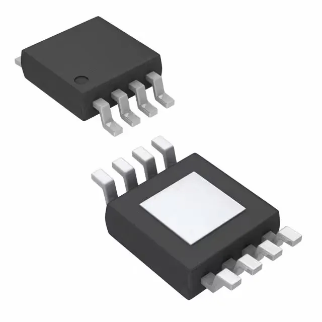
8-HVSSOP with PowerPad — thermal and layout notes
Without the via stitch, thermal resistance rises significantly and the device may hit thermal shutdown above 85°C ambient. The exposed pad also provides a low-inductance return path for the high-frequency output currents, which helps control radiated emissions. The package footprint is 3.00 mm × 3.00 mm (0.118" × 0.118"), matching the standard 8-MSOP land pattern with the centre pad added.
TI lists the SN65LVDS9638DGN as Active. For dual-sourcing or second-source qualification, the 65LVDS family includes the SN65LVDS9638D (the same die in a standard 8-SOIC package) — the DGN variant is the smaller HVSSOP footprint with the exposed pad, not a functional alternative. If your board already routes to the 8-HVSSOP land pattern, stick with the DGN suffix.