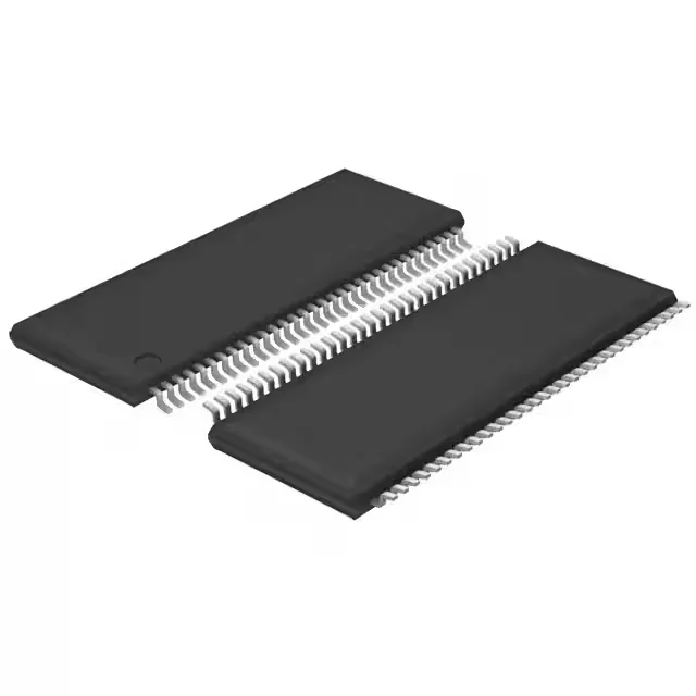
Quad LVDS receiver for 250 Mbps point-to-point links
The Texas Instruments SN65LVDS386DGGG4 is a quad-channel LVDS receiver in the 65LVDS family, designed to convert differential LVDS signals into single-ended CMOS outputs at data rates up to 250 Mbps per channel. With four receivers and no drivers on-chip (0/4 driver/receiver count), it is a pure receive-side device for applications such as clock distribution, backplane interconnects, and cable extension in industrial or telecom equipment.
The 250 Mbps data rate per receiver is the maximum toggle rate the input stage can reliably recover from a differential LVDS signal. In practice, this supports common serial protocols like SPI-over-LVDS or parallel bus deserialization at 250 MHz DDR clock rates. The receiver's input threshold and hysteresis are specified for LVDS levels (typically 350 mV swing), so the signal source must meet the LVDS standard — not CML or LVPECL — without external level shifting. At 250 Mbps, the 64-TSSOP package's lead inductance and trace stub lengths become significant; keep the differential pair impedance at 100 Ω and route the pair tightly to the receiver inputs.
The base product number 65LVDS386 covers the family, so PCN notifications for package or wafer changes would apply across the 65LVDS386 variants.
64-TSSOP footprint and supply routing
The 64-TFSOP (0.240", 6.10mm width) package is the thin-shrink small-outline variant with a 0.5 mm lead pitch, surface-mount only. The supplier device package is 64-TSSOP. For decoupling, place a 0.1 µF ceramic capacitor close to each supply pin pair (VCC/GND) — the 3V to 3.6V rail should be clean to within 100 mV peak-to-peak at 250 Mbps to avoid jitter on the recovered CMOS output.