What this LVDS reDriver does on the board
It accepts a differential input and outputs a reconditioned LVDS signal, compensating for cable and PCB attenuation at data rates up to 4 Gbps. Typical deployment is in backplane, cable extension, and clock distribution applications where the eye diagram would otherwise close before the receiver. The 30 ns propagation delay must be budgeted in the system timing — it is not a zero-delay repeater, so the total path delay from source to load includes this reDriver latency.
The 4 Gbps maximum data rate places this reDriver in the high-speed serial lane class. At that rate, the fundamental frequency component is 2 GHz, and the 3 dB bandwidth needed for a clean eye is roughly 2.8 GHz. The 30 ns delay is fixed and independent of data rate, so at 4 Gbps the delay represents 120 unit intervals — well within the typical CDR tracking range for most SerDes receivers, but worth verifying if the link uses a non-standard protocol with a narrow lock window. The differential input and LVDS output are both standard 100 Ω termination schemes. No external bias resistors are needed for the output — the reDriver provides the correct LVDS output levels directly. The 35 mA supply current is the total for the single channel, including the input termination and output drive.
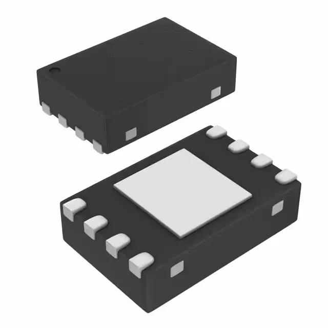
Package and footprint — 8-WSON with exposed pad
The SN65LVDS20DRFR comes in an 8-WFDFN exposed-pad package, also designated as 8-WSON with a 2 mm x 2 mm body. The pad also provides a low-inductance ground return for the high-speed signal path. Surface-mount assembly is standard. The small 2x2 mm footprint leaves room for the decoupling capacitor close to the supply pin, which is critical at 4 Gbps to minimize supply ripple coupling into the output jitter.