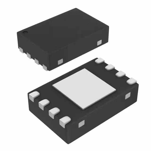
PECL-to-LVDS signal conditioner in a 2x2 mm package
It is designed for high-speed serial links where signal integrity degrades over backplane traces or cables — the reDriver reshapes the edge rates and re-transmits a clean LVDS swing, effectively extending the reach of a PECL source without a separate PLL or retimer. Rated for a maximum data rate of 2 Gbps with a typical propagation delay of 460 ps, the part fits 1 GbE, SATA Gen 1, and general-purpose clock/data distribution up to 2 Gbps.
The closest pin-compatible alternative in the same functional family would be the SN65LVDS18 (non-RG4 suffix) or a cross from a second-source vendor such as Onsemi or Microchip — but each has its own supply and temperature-grade profile. Validate the replacement against your signal-level and timing budget before committing the BOM line.
Signal translation and timing budget
The PECL input threshold is referenced to a 3.3 V or 2.5 V PECL swing; the LVDS output drives a 100 Ω differential termination with a typical 350 mV swing. The 460 ps propagation delay adds to the overall link latency — budget it in your timing closure for source-synchronous interfaces where the clock and data paths must match within a few hundred picoseconds. The single-channel topology means one PECL pair in, one LVDS pair out. For multi-drop or multi-lane applications, you need one device per lane. The 2 Gbps data rate is the maximum specified — derate for cable losses or connector discontinuities; the reDriver does not recover the clock, so jitter accumulates across cascaded stages.