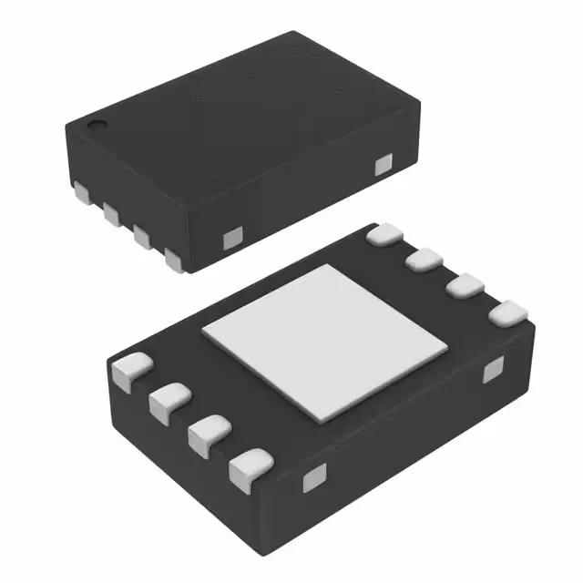
PECL-to-LVDS buffer/re-driver for 4 Gbps serial links
It is designed to clean up and retransmit high-speed differential signals — think clock distribution, serial backplane links, or data paths in telecom and industrial equipment where the trace runs get long enough to degrade the edge. The part handles data rates up to 4 Gbps and adds only 460 ps of propagation delay, so it fits into a timing budget without forcing a re-spin of the clock tree. Supply range is 2.375 V to 3.6 V, which lets it run off a common 2.5 V or 3.3 V rail without a separate regulator.
The 460 ps typical delay is the time the signal spends inside the part. In a multi-drop clock tree, every buffer stage adds skew; at 4 Gbps a bit period is 250 ps, so this delay is about two bit-times. That is tight enough that you need to account for it in the timing closure spreadsheet, but it will not blow the margin on a well-designed board. The 4 Gbps data rate covers common serial standards like 10GBASE-KR, CPRI, and JESD204B at their lane rates. If the system runs at 3.125 Gbps or lower, the margin is even wider.
Package and footprint — 8-WSON with exposed pad
The part comes in an 8-WFDFN with exposed pad, also called 8-WSON (2x2 mm). The small footprint (2x2 mm) is a plus on dense boards, but the pad is not visible from the top, so orientation relies on pin-1 marking. No lab, no bench — just a good pair of tweezers and a steady hand on the reflow profile.
Active lifecycle — no LTB worry
If a second source is needed for dual-supply resilience, the base product number 65LVDS16 is shared across the family, so a pin-compatible variant in a different tape/reel option is the natural cross-reference.